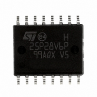
M25P128-VMF6P NUMONYX, M25P128-VMF6P Datasheet - Page 33

M25P128-VMF6P
Manufacturer Part Number
M25P128-VMF6P
Description
IC FLASH 128MBIT 50MHZ 16SOIC
Manufacturer
NUMONYX
Series
Forté™r
Datasheet
1.M25P128-VME6TGB.pdf
(47 pages)
Specifications of M25P128-VMF6P
Format - Memory
FLASH
Memory Type
FLASH
Memory Size
128M (16M x 8)
Speed
50MHz
Interface
SPI, 3-Wire Serial
Voltage - Supply
2.7 V ~ 3.6 V
Operating Temperature
-40°C ~ 85°C
Package / Case
16-SOIC
Cell Type
NOR
Density
128Mb
Access Time (max)
8ns
Interface Type
Serial (SPI)
Boot Type
Not Required
Address Bus
1b
Operating Supply Voltage (typ)
3.3V
Operating Temp Range
-40C to 85C
Package Type
SO W
Sync/async
Synchronous
Operating Temperature Classification
Industrial
Operating Supply Voltage (min)
2.7V
Operating Supply Voltage (max)
3.6V
Word Size
8b
Number Of Words
16M
Supply Current
8mA
Mounting
Surface Mount
Pin Count
16
Lead Free Status / RoHS Status
Lead free / RoHS Compliant
Other names
Q2855929
Q3097367
Q3097367
Available stocks
Company
Part Number
Manufacturer
Quantity
Price
Part Number:
M25P128-VMF6P
Manufacturer:
ST
Quantity:
20 000
Company:
Part Number:
M25P128-VMF6PB
Manufacturer:
CIRRUS
Quantity:
320
Part Number:
M25P128-VMF6PB
Manufacturer:
ST
Quantity:
20 000
Company:
Part Number:
M25P128-VMF6PB,M25P128-VMF6TP
Quantity:
70
8
Figure 18. Power-up timing
Table 8.
1. 65 nm technology devices are identified by the process identification digit ‘A’ in the device marking and
2. These parameters are characterized only.
Table 9.
1. These parameters are characterized only.
Initial delivery state
The device is delivered with the memory array erased: all bits are set to 1 (each byte
contains FFh). The Status Register contains 00h (all Status Register bits are 0).
Symbol
Symbol
V CC (max)
t
t
V CC (min)
t
t
PUW
PUW
VSL
VSL
V
process letter "B" in the part number.
V
WI
WI
(2)
(1)
(2)
(2)
V WI
V CC
V
Time delay to Write instruction
Write Inhibit Voltage
V
Time delay to Write instruction
Write Inhibit Voltage
CC
CC
Reset State
Power-up timing and V
Power-up timing and V
Device
(min) to S Low
(min) to S Low
of the
Program, Erase and Write Commands are Rejected by the Device
Chip Selection Not Allowed
Parameter
Parameter
WI
WI
threshold for 65 nm devices
threshold for 130 nm devices
tPUW
tVSL
Read Access allowed
Min.
Min.
200
400
1.5
1.5
60
(1)
1
Device fully
accessible
Max.
Max.
2.5
10
2.5
time
AI04009C
Unit
Unit
ms
33/47
µs
µs
µs
V
V


