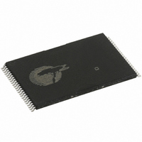
CY62167DV30LL-45ZXIT Cypress Semiconductor Corp, CY62167DV30LL-45ZXIT Datasheet

CY62167DV30LL-45ZXIT
Specifications of CY62167DV30LL-45ZXIT
Related parts for CY62167DV30LL-45ZXIT
CY62167DV30LL-45ZXIT Summary of contents
Page 1
... Power-Down Circuit Note: 1. For best-practice recommendations, please refer to the Cypress application note “System Design Guidelines” on http://www.cypress.com. Cypress Semiconductor Corporation Document #: 38-05328 Rev. *G 16-Mbit (1M x 16) Static RAM also has an automatic power-down feature that significantly reduces power consumption by 99% when addresses are not toggling ...
Page 2
... Product Portfolio V Range (V) CC Product Min. Typ. CY62167DV30LL 2.2 3.0 [ Pin Configuration A15 1 A14 2 A13 3 A12 4 A11 5 A10 A19 CE2 12 DNU 13 BHE 14 BLE 15 A18 16 A17 Notes: 2. Typical values are included for reference only and are not guaranteed or tested. Typical values are measured ...
Page 3
... Full Device AC operation requires linear V CC Document #: 38-05328 Rev. *G Output Current into Outputs (LOW) .............................20 mA Static Discharge Voltage .......................................... > 2001V (per MIL-STD-883, Method 3015) Latch-up Current .....................................................> 200 mA Operating Range + 0.3V Device CC CY62167DV30LL Industrial + 0. 0.3V CC CY62167DV30-45 CY62167DV30-55 CY62167DV30-70 [2] Test Conditions Min. Typ 2.20V 2 ...
Page 4
Capacitance Parameter Description C Input Capacitance IN C Output Capacitance OUT [10] Thermal Resistance Parameter Description Θ Thermal Resistance JA (Junction to Ambient) Θ Thermal Resistance JC (Junction to Case) AC Test Loads and Waveforms ...
Page 5
... HZCE HZBE HZWE 18. The internal Write time of the memory is defined by the overlap of WE write and any of these signals can terminate a write by going INACTIVE. The data input set-up and hold timing should be referenced to the edge of the signal that terminates the Write. Document #: 38-05328 Rev. *G DATA RETENTION MODE > ...
Page 6
Switching Waveforms Read Cycle 1 (Address Transition Controlled) ADDRESS PREVIOUS DATA VALID DATA OUT [20, 21] Read Cycle 2 (OE Controlled) ADDRESS BHE/BLE t LZBE OE HIGH IMPEDANCE DATA OUT t LZCE ...
Page 7
Switching Waveforms (continued) [18, 22, 23, 24] Write Cycle 1 (WE Controlled) ADDRESS BHE/BLE OE DATA I/O See Note 23 t HZOE Notes: 22. Data I/O is high-impedance ...
Page 8
Switching Waveforms (continued) Write Cycle 2 ( Controlled ADDRESS BHE/BLE OE DATA I/O See Note 23 t HZOE Write Cycle 3 (WE Controlled, OE LOW) ADDRESS BHE/BLE ...
Page 9
Switching Waveforms (continued) Write Cycle 4 (BHE/BLE Controlled, OE LOW) ADDRESS BHE/BLE See Note 23 DATA I/O Truth Table BHE ...
Page 10
... Ordering Information Speed Ordering Code (ns) 45 CY62167DV30LL-45ZXI 55 CY62167DV30LL-55BVI CY62167DV30LL-55BVXI CY62167DV30LL-55ZI CY62167DV30LL-55ZXI 70 CY62167DV30LL-70BVI Please contact your local Cypress sales representative for availability of these parts Package Diagrams TOP VIEW A1 CORNER 8.00±0.10 SEATING PLANE C Document #: 38-05328 Rev. *G Package Package Type Diagram 51-85183 48-pin TSOP I ( mm) (Pb-free) 51-85178 48-ball Fine Pitch BGA ( ...
Page 11
... Document #: 38-05328 Rev. *G © Cypress Semiconductor Corporation, 2006. The information contained herein is subject to change without notice. Cypress Semiconductor Corporation assumes no responsibility for the use of any circuitry other than circuitry embodied in a Cypress product. Nor does it convey or imply any license under patent or other rights. Cypress products are not warranted nor intended to be used for medical, life support, life saving, critical control or safety applications, unless pursuant to an express written agreement with Cypress ...
Page 12
Document History Page Document Title: CY62167DV30 MoBL Document Number: 38-05328 REV. ECN NO. Issue Date ** 118408 09/30/02 *A 123692 02/11/03 *B 126555 04/25/03 *C 127841 09/10/03 *D 205701 *E 238050 See ECN *F 304054 See ECN *G 492895 See ...


