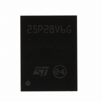
M25P128-VME6G NUMONYX, M25P128-VME6G Datasheet - Page 24

M25P128-VME6G
Manufacturer Part Number
M25P128-VME6G
Description
IC FLASH 128MBIT 50MHZ 8VDFPN
Manufacturer
NUMONYX
Series
Forté™r
Datasheet
1.M25P128-VME6TGB.pdf
(47 pages)
Specifications of M25P128-VME6G
Format - Memory
FLASH
Memory Type
FLASH
Memory Size
128M (16M x 8)
Speed
50MHz
Interface
SPI, 3-Wire Serial
Voltage - Supply
2.7 V ~ 3.6 V
Operating Temperature
-40°C ~ 85°C
Package / Case
8-VDFPN
Cell Type
NOR
Density
128Mb
Access Time (max)
8ns
Interface Type
Serial (SPI)
Boot Type
Not Required
Address Bus
1b
Operating Supply Voltage (typ)
3.3V
Operating Temp Range
-40C to 85C
Package Type
VDFPN EP
Sync/async
Synchronous
Operating Temperature Classification
Industrial
Operating Supply Voltage (min)
2.7V
Operating Supply Voltage (max)
3.6V
Word Size
8b
Number Of Words
16M
Supply Current
8mA
Mounting
Surface Mount
Pin Count
8
Lead Free Status / RoHS Status
Lead free / RoHS Compliant
Available stocks
Company
Part Number
Manufacturer
Quantity
Price
Part Number:
M25P128-VME6G
Manufacturer:
MICRON/镁光
Quantity:
20 000
Company:
Part Number:
M25P128-VME6GB
Manufacturer:
NUMONYX
Quantity:
1 920
Company:
Part Number:
M25P128-VME6GB
Manufacturer:
SILICON
Quantity:
2 310
Part Number:
M25P128-VME6GB
Manufacturer:
ST
Quantity:
20 000
6.5
24/47
Write status register (WRSR)
The Write Status Register (WRSR) instruction allows new values to be written to the Status
Register. Before it can be accepted, a Write Enable (WREN) instruction must previously
have been executed. After the Write Enable (WREN) instruction has been decoded and
executed, the device sets the Write Enable Latch (WEL).
The Write Status Register (WRSR) instruction is entered by driving Chip Select (S) Low,
followed by the instruction code and the data byte on Serial Data Input (D).
The instruction sequence is shown in
The Write Status Register (WRSR) instruction has no effect on b6, b5, b1 and b0 of the
Status Register. b6 and b5 are always read as 0.
Chip Select (S) must be driven High after the eighth bit of the data byte has been latched in.
If not, the Write Status Register (WRSR) instruction is not executed. As soon as Chip Select
(S) is driven High, the self-timed Write Status Register cycle (whose duration is t
initiated. While the Write Status Register cycle is in progress, the Status Register may still
be read to check the value of the Write In Progress (WIP) bit. The Write In Progress (WIP)
bit is 1 during the self-timed Write Status Register cycle, and is 0 when it is completed.
When the cycle is completed, the Write Enable Latch (WEL) is reset.
The Write Status Register (WRSR) instruction allows the user to change the values of the
Block Protect (BP2, BP1, BP0) bits, to define the size of the area that is to be treated as
read-only, as defined in
the user to set or reset the Status Register Write Disable (SRWD) bit in accordance with the
Write Protect (W/V
Protect (W/V
The Write Status Register (WRSR) instruction is not executed once the Hardware Protected
Mode (HPM) is entered.
Table 7.
1. As defined by the values in the Block Protect (BP2, BP1, BP0) bits of the Status Register, as shown in
The protection features of the device are summarized in
When the Status Register Write Disable (SRWD) bit of the Status Register is 0 (its initial
delivery state), it is possible to write to the Status Register provided that the Write Enable
W/V
Signal
Table 2: Protected area
1
0
1
0
PP
SRWD
Bit
0
0
1
1
PP
Protection modes
) signal allow the device to be put in the Hardware Protected Mode (HPM).
Protected
Hardware
Protected
Software
(SPM)
(HPM)
PP
Mode
) signal. The Status Register Write Disable (SRWD) bit and Write
sizes.
Table
Status Register is Writable
(if the WREN instruction
has set the WEL bit)
The values in the SRWD,
BP2, BP1 and BP0 bits
can be changed
Status Register is
Hardware write protected
The values in the SRWD,
BP2, BP1 and BP0 bits
cannot be changed
Write Protection of the
2. The Write Status Register (WRSR) instruction also allows
Status Register
Figure
12.
Protected against
Page Program,
Sector Erase and
Bulk Erase
Protected against
Page Program,
Sector Erase and
Bulk Erase
Protected Area
Table 7
Memory Content
(1)
Ready to accept
Page Program and
Sector Erase
instructions
Ready to accept
Page Program and
Sector Erase
instructions
Unprotected Area
W
) is
(1)


