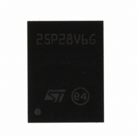
M25P128-VME6G NUMONYX, M25P128-VME6G Datasheet - Page 8

M25P128-VME6G
Manufacturer Part Number
M25P128-VME6G
Description
IC FLASH 128MBIT 50MHZ 8VDFPN
Manufacturer
NUMONYX
Series
Forté™r
Datasheet
1.M25P128-VME6TGB.pdf
(47 pages)
Specifications of M25P128-VME6G
Format - Memory
FLASH
Memory Type
FLASH
Memory Size
128M (16M x 8)
Speed
50MHz
Interface
SPI, 3-Wire Serial
Voltage - Supply
2.7 V ~ 3.6 V
Operating Temperature
-40°C ~ 85°C
Package / Case
8-VDFPN
Cell Type
NOR
Density
128Mb
Access Time (max)
8ns
Interface Type
Serial (SPI)
Boot Type
Not Required
Address Bus
1b
Operating Supply Voltage (typ)
3.3V
Operating Temp Range
-40C to 85C
Package Type
VDFPN EP
Sync/async
Synchronous
Operating Temperature Classification
Industrial
Operating Supply Voltage (min)
2.7V
Operating Supply Voltage (max)
3.6V
Word Size
8b
Number Of Words
16M
Supply Current
8mA
Mounting
Surface Mount
Pin Count
8
Lead Free Status / RoHS Status
Lead free / RoHS Compliant
Available stocks
Company
Part Number
Manufacturer
Quantity
Price
Part Number:
M25P128-VME6G
Manufacturer:
MICRON/镁光
Quantity:
20 000
Company:
Part Number:
M25P128-VME6GB
Manufacturer:
NUMONYX
Quantity:
1 920
Company:
Part Number:
M25P128-VME6GB
Manufacturer:
SILICON
Quantity:
2 310
Part Number:
M25P128-VME6GB
Manufacturer:
ST
Quantity:
20 000
2
2.1
2.2
2.3
2.4
2.5
8/47
Signal description
Serial data output (Q)
This output signal is used to transfer data serially out of the device. Data is shifted out on the
falling edge of Serial Clock (C).
Serial data input (D)
This input signal is used to transfer data serially into the device. It receives instructions,
addresses, and the data to be programmed. Values are latched on the rising edge of Serial
Clock (C).
Serial clock (C)
This input signal provides the timing of the serial interface. Instructions, addresses, or data
present at Serial Data Input (D) are latched on the rising edge of Serial Clock (C). Data on
Serial Data Output (Q) changes after the falling edge of Serial Clock (C).
Chip Select (S)
When this input signal is High, the device is deselected and Serial Data Output (Q) is at high
impedance. Unless an internal Program, Erase or Write Status Register cycle is in progress,
the device will be in the Standby Power mode. Driving Chip Select (S) Low selects the
device, placing it in the Active Power mode.
After Power-up, a falling edge on Chip Select (S) is required prior to the start of any
instruction.
Hold (HOLD)
The Hold (HOLD) signal is used to pause any serial communications with the device without
deselecting the device.
During the Hold condition, the Serial Data Output (Q) is high impedance, and Serial Data
Input (D) and Serial Clock (C) are Don’t Care.
To start the Hold condition, the device must be selected, with Chip Select (S) driven Low.


