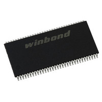
W9412G6IH-5 Winbond Electronics, W9412G6IH-5 Datasheet - Page 12

W9412G6IH-5
Manufacturer Part Number
W9412G6IH-5
Description
IC DDR-400 SDRAM 128MB 66TSSOPII
Manufacturer
Winbond Electronics
Datasheet
1.W9412G6IH-5.pdf
(53 pages)
Specifications of W9412G6IH-5
Format - Memory
RAM
Memory Type
DDR SDRAM
Memory Size
128M (8Mx16)
Speed
250MHz
Interface
Parallel
Voltage - Supply
2.3 V ~ 2.7 V
Operating Temperature
0°C ~ 70°C
Package / Case
66-TSOPII
Lead Free Status / RoHS Status
Lead free / RoHS Compliant
Available stocks
Company
Part Number
Manufacturer
Quantity
Price
Part Number:
W9412G6IH-5
Manufacturer:
WINBOND/华邦
Quantity:
20 000
7.2.14 Self Refresh Entry Command
7.2.15 Self Refresh Exit Command
7.2.16 Data Write Enable /Disable Command
7.3
To allow for improved efficiency in scheduling and switching between tasks, some flexibility in the
absolute refresh interval is provided. A maximum of eight AUTO REFRESH commands can be
posted to any given DDR SDRAM, and the maximum absolute interval between any AUTO
REFRESH command and the next AUTO REFRESH command is 8 * t
( RAS = “L”, CAS = “L”, WE = “H”, CKE = “L”, BA0, BA1, A0 to A11 = Don’t Care)
The SELF REFRESH command can be used to retain data in the DDR SDRAM, even if the rest of
the system is powered down. When in the self refresh mode, the DDR SDRAM retains data
without external clocking. The SELF REFRESH command is initiated like an AUTO REFRESH
command except CKE is disabled (LOW). The DLL is automatically disabled upon entering SELF
REFRESH, and is automatically enabled upon exiting SELF REFRESH. Any time the DLL is
enabled a DLL Reset must follow and 200 clock cycles should occur before a READ command
can be issued. Input signals except CKE are “Don’t Care” during SELF REFRESH. Since CKE is a
SSTL_2 input,
(CKE = “H”, CS = “H” or CKE = “H”, RAS = “H”, CAS = “H”)
The procedure for exiting self refresh requires a sequence of commands. First, CLK must be
stable prior to CKE going back HIGH. Once CKE is HIGH, the DDR SDRAM must have NOP
commands issued for t
progress. A simple algorithm for meeting both refresh and DLL requirements is to apply NOPs for
200 clock cycles before applying any other command.
The use of SELF REFREH mode introduces the possibility that an internally timed event can be
missed when CKE is raised for exit from self refresh mode. Upon exit from SELF REFRESH an
extra auto refresh command is recommended.
(DM = “L/H” or LDM, UDM = “L/H”)
During a Write cycle, the DM or LDM, UDM signal functions as Data Mask and can control every
word of the input data. The LDM signal controls DQ0 to DQ7 and UDM signal controls DQ8 to
DQ15.
Issuing the Bank Activate command to the idle bank puts it into the active state. When the Read
command is issued after t
synchronized with both edges of DQS (Burst Read operation). The initial read data becomes
available after CAS Latency from the issuing of the Read command. The CAS Latency must be set
in the Mode Register at power-up.
When the Precharge Operation is performed on a bank during a Burst Read and operation, the
Burst operation is terminated.
When the Read with Auto-precharge command is issued, the Precharge operation is performed
automatically after the Read cycle then the bank is switched to the idle state. This command
cannot be interrupted by any other commands. Refer to the diagrams for Read operation.
FRESH cycles at an average periodic interval of t
Read Operation
V
REF
must be maintained during SELF REFRESH.
XSNR
RCD
because time is required for the completion of any internal refresh in
from the Bank Activate command, the data is read out sequentially,
- 12 -
REFI
(maximum).
Publication Release Date: Sep. 16, 2009
REFI
.
W9412G6IH
Revision A06


