AT17C512-10JC Atmel, AT17C512-10JC Datasheet - Page 2
AT17C512-10JC
Manufacturer Part Number
AT17C512-10JC
Description
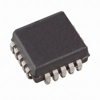
IC SER CONFIG PROM 512K 20PLCC
Manufacturer
Atmel
Datasheet
1.AT17C512-10JC.pdf
(13 pages)
Specifications of AT17C512-10JC
Programmable Type
Serial EEPROM
Memory Size
512kb
Voltage - Supply
4.75 V ~ 5.25 V
Operating Temperature
0°C ~ 70°C
Package / Case
20-LCC (J-Lead)
Lead Free Status / RoHS Status
Contains lead / RoHS non-compliant
Available stocks
Company
Part Number
Manufacturer
Quantity
Price
Company:

Part Number:
AT17C512-10JC
Manufacturer:
ATM
Quantity:
1 980
Company:
Part Number:
AT17C512-10JC
Manufacturer:
ATM
Quantity:
129
Company:
Part Number:
AT17C512-10JC
Manufacturer:
ATM
Quantity:
1 980
Company:
Part Number:
AT17C512-10JC
Manufacturer:
PHI
Quantity:
6 221
Part Number:
AT17C512-10JC
Manufacturer:
ATMEL/爱特梅尔
Quantity:
20 000


Block Diagram
FPGA Master Serial
Mode Summary
Controlling the High-
density AT17 Series
Serial EEPROMs
During Configuration
2
AT17C512/010/LV512/010
The I/O and logic functions of the FPGA and their associated interconnections are
established by a configuration program. The program is loaded either automatically
upon power-up, or on command, depending on the state of the FPGA mode pins. In
Master Mode, the FPGA automatically loads the configuration program from an external
memory. The AT17 Serial Configuration EEPROM has been designed for compatibility
with the Master Serial Mode.
This document discusses the AT40K FPGA interface. For more details or AT6000
FPGA applications, please reference “AT40K Series Configuration” or “AT6000 Series
Configuration” application notes.
Most connections between the FPGA device and the AT17 Serial Configuration
EEPROM are simple and self-explanatory:
The DATA output of the AT17 Series Configurator drives DIN of the FPGA devices.
The master FPGA CCLK output drives the CLK input of the AT17 Series Configurator.
The CEO output of any AT17C/LV512/010 drives the CE input of the next
AT17C/LV512/010 in a cascade chain of EEPROMs.
SER_EN must be connected to VCC (except during ISP).
The READY pin is available as an open-collector indicator of the device’s reset status; it
is driven Low while the device is in its power-on reset cycle and released (tri-stated)
when the cycle is complete. This pin is not available in the 8-pin package.
There are two different ways to use the inputs CE and OE.
Related parts for AT17C512-10JC
Image
Part Number
Description
Manufacturer
Datasheet
Request
R

Part Number:
Description:
IC SER CONFIG PROM 512K 20PLCC
Manufacturer:
Atmel
Datasheet:

Part Number:
Description:
IC SRL CONFIG EEPROM 512K 8LAP
Manufacturer:
Atmel
Datasheet:

Part Number:
Description:
IC SRL CONFIG EEPROM 512K 20PLCC
Manufacturer:
Atmel
Datasheet:
Part Number:
Description:
IC SRL CONFIG EEPROM 512K 8LAP
Manufacturer:
Atmel
Datasheet:
Part Number:
Description:
IC SRL CONFIG EEPROM 512K 20PLCC
Manufacturer:
Atmel
Datasheet:

Part Number:
Description:
DEV KIT FOR AVR/AVR32
Manufacturer:
Atmel
Datasheet:

Part Number:
Description:
INTERVAL AND WIPE/WASH WIPER CONTROL IC WITH DELAY
Manufacturer:
ATMEL Corporation
Datasheet:
Part Number:
Description:
Low-Voltage Voice-Switched IC for Hands-Free Operation
Manufacturer:
ATMEL Corporation
Datasheet:
Part Number:
Description:
MONOLITHIC INTEGRATED FEATUREPHONE CIRCUIT
Manufacturer:
ATMEL Corporation
Datasheet:
Part Number:
Description:
AM-FM Receiver IC U4255BM-M
Manufacturer:
ATMEL Corporation
Datasheet:
Part Number:
Description:
Monolithic Integrated Feature Phone Circuit
Manufacturer:
ATMEL Corporation
Datasheet:
Part Number:
Description:
Multistandard Video-IF and Quasi Parallel Sound Processing
Manufacturer:
ATMEL Corporation
Datasheet: