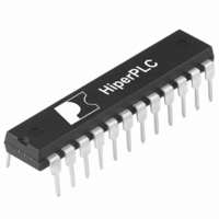
PLC810PG Power Integrations, PLC810PG Datasheet - Page 5

PLC810PG
Manufacturer Part Number
PLC810PG
Description
IC OFFLINE CTRLR CM OCP HV 24DIP
Manufacturer
Power Integrations
Series
HiperPLC™r
Datasheet
1.PLC810PG.pdf
(26 pages)
Specifications of PLC810PG
Output Isolation
Isolated
Frequency Range
50 ~ 300kHz
Voltage - Input
8.1 ~ 15 V
Voltage - Output
600V
Power (watts)
700mW
Operating Temperature
-40°C ~ 125°C
Package / Case
24-DIP (0.300", 7.62mm)
Switching Frequency
300 KHz
Maximum Power Dissipation
700 mW
Mounting Style
Through Hole
For Use With
596-1265 - KIT REF DESIGN FOR PLC810
Lead Free Status / RoHS Status
Lead free / RoHS Compliant
Other names
596-1264-5
Available stocks
Company
Part Number
Manufacturer
Quantity
Price
Company:
Part Number:
PLC810PG
Manufacturer:
POWER
Quantity:
15 000
Part Number:
PLC810PG
Manufacturer:
POWER
Quantity:
20 000
Block Diagram
Figure 3 shows a block diagram of the functional elements that
make up the PLC810PG. The reserved pins are not shown in
the diagram. Those pins are reserved for PI use during
manufacture and testing. The PLC810PG PFC control blocks
and circuits are shown on the upper half of the block diagram,
while the LLC control blocks are shown on the lower half. Some
of the functional blocks are shared.
PLC810PG Power Block
The PLC810PG is powered through VCC and VCCL pins. The
VCCL pin powers the LLC driver while VCC powers the rest of the
device. VCC pin must be supplied by a voltage between V
Figure 3.
www.powerint.com
VCOMP (1)
GND (2,19)
FMAX (21)
Block Diagram of PLC810PG. Reserved Pins are not Shown.
FBP (23)
FBL (20)
ISL (22)
ISP (3)
V
REF
V
INVERSION
FBPREF
LLC CURRENT
START
FEEDBACK
SOFT
V
V
SD(H)
IN(H)
V
ISL(F)
+
OTA
-
V
/V
V
SD(L)
ONE SHOT
OVH
IN(L)
V
CYCLES
ISL(S)
4096
V
OC
+
+
+
-
-
-
and LPF
DVGA
+
-
+
PFC INHIBIT
1.2 V
-
RAMP AND CLOCK
OV FAULT
LLC OFF
INTERNAL REFERENCE
GENERATOR
GENERATOR
DEAD TIME
OC FAULT
OVL FAULT
LLC OFF
CLAMP
GENERATOR
+
-
UVLO(+)
LLC CLOCK
CLAMP
OVL FAULT
ALIGNMENT
and 15 V. The provided supply is continuously compared against
the V
When VCC is above the V
asserts the undervoltage lockout (UVLO) signal allowing the device
to start. If VCC falls below V
shutting down the PLC810PG.
The VCCL pin powers the LLC driver, and VCCHB provides the
charge for the LLC high-side MOSFET for gate drive.
An internal linear regulator is used to generate a 3.3 V rail to power
the low voltage circuits inside the PLC810PG. The 3.3 V is brought
outside on the VREF pin allowing external low voltage circuits to be
powered by the PLC810PG.
PHASE
GENERATOR
PWM
OVERLAP
LLC FAULT
UVLO(+)
NON-
and V
UVLO
UVLO(-)
thresholds to start/stop the PLC810PG.
UVLO(+)
RESET
UVLO(-)
3.3 V LINEAR
+
REGULATOR
-
threshold the PLC810PG de-
, the UVLO signal is asserted,
V
V
UVLO(+)
UVLO(-)
PLC810PG
(6) GATEP
(7) VCC
(8) GNDP
(4) VREF
(13) VCCHB
(12) GATEH
(14) HB
(16) VCCL
(10) GATEL
(9) GNDL
PI-5041-112608
Rev. F 08/09
5


