TOP104YN Power Integrations, TOP104YN Datasheet - Page 6
TOP104YN
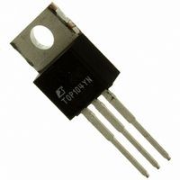
Manufacturer Part Number
TOP104YN
Description
IC OFFLINE SWIT PWM OTP HV TO220
Manufacturer
Power Integrations
Series
TOPSwitch®r
Datasheet
1.TOP104YN.pdf
(18 pages)
Specifications of TOP104YN
Output Isolation
Isolated
Frequency Range
90 ~ 110kHz
Voltage - Output
350V
Power (watts)
110W
Operating Temperature
-40°C ~ 150°C
Package / Case
TO-220-3
Output Voltage
5.8 V
Input / Supply Voltage (max)
110 VAC
Input / Supply Voltage (min)
100 VAC
Duty Cycle (max)
70 %
Switching Frequency
100 KHz
Supply Current
1.2 mA
Operating Temperature Range
- 40 C to + 150 C
Mounting Style
Through Hole
Lead Free Status / RoHS Status
Lead free / RoHS Compliant
Other names
596-1148-5
TOP104YN
TOP104YN
Available stocks
Company
Part Number
Manufacturer
Quantity
Price
Company:

Part Number:
TOP104YN
Manufacturer:
POWER
Quantity:
12 000
Part Number:
TOP104YN
Manufacturer:
POWER
Quantity:
20 000


General Circuit Operation
Primary Feedback Regulation
The circuit shown in Figure 7 is a simple
5 V, 5 W bias supply using the TOP100.
This flyback power supply employs
primary-side regulation from a
transformer bias winding. This approach
is best for low-cost applications requiring
isolation and operation within a narrow
range of load variation. Line and load
regulation of
achieved from 10% to 100% of rated
load.
Voltage feedback is obtained from the
transformer (T1) bias winding, which
eliminates the need for optocoupler and
secondary-referenced error amplifier.
High-voltage DC is applied to the
primary winding of T1. The other side
of the transformer primary is driven by
Figure 7. Schematic Diagram of a Minimum Parts Count 5 V, 5 W Bias Supply Utilizing the TOP100.
6
TOP100-4
F
7 /09
INPUT
DC
5% or better can be
CONTROL
SOURCE
DRAIN
TOP100YAI
U1
the integrated high-voltage MOSFET
transistor within the TOP100 (U1). The
circuit operates at a switching frequency
of 100 kHz, set by the internal oscillator
of the TOP100. The clamp circuit
implemented by VR1 and D1 limits the
leading-edge voltage spike caused by
transformer leakage inductance to a safe
value. The 5 V power secondary winding
is rectified and filtered by D2, C2, C3,
and L1 to create the 5 V output voltage.
The output of the T1 bias winding is
rectified and filtered by D3, R1, and C5.
The voltage across C5 is regulated by
U1, and is determined by the 5.7 V
internal shunt regulator at the
CONTROL pin of U1.
rectified bias voltage on C5 begins to
exceed the shunt regulator voltage,
P6KE91
UF4004
VR1
47 F
D1
C5
T1
When the
22
R1
1N5822
D2
1N4148
330 F
D3
25 V
C2
current will flow into the control pin.
Increasing control pin current decreases
the duty cycle until a stable operating
point is reached. The output voltage is
proportional to the bias voltage by the
turns ratio of the output to bias windings.
C5 is used to bypass the CONTROL pin.
C5 also provides loop compensation for
the power supply by shunting AC
currents around the CONTROL pin
dynamic impedance, and also determines
the auto-restart frequency during start-
up and auto-restart conditions. See DN-
8 for more information regarding bias
supplies.
(Bead)
CIRCUIT PERFORMANCE:
L1
Line Regulation - ±1.5%
150 F
Ripple Voltage ±25 mV
Load Regulation - ±4%
25 V
C3
95 to 185 V DC
(10% to 100%)
PI-1767-020296
5 V
RTN
Related parts for TOP104YN
Image
Part Number
Description
Manufacturer
Datasheet
Request
R

Part Number:
Description:
SOP-16
Manufacturer:
Power Integrations
Datasheet:
Part Number:
Description:
DIP8
Manufacturer:
Power Integrations
Datasheet:
Part Number:
Description:
TO-263
Manufacturer:
Power Integrations
Datasheet:
Part Number:
Description:
TO-263
Manufacturer:
Power Integrations
Datasheet:
Part Number:
Description:
Manufacturer:
Power Integrations
Datasheet: