TOP104YN Power Integrations, TOP104YN Datasheet - Page 7
TOP104YN
Manufacturer Part Number
TOP104YN
Description
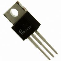
IC OFFLINE SWIT PWM OTP HV TO220
Manufacturer
Power Integrations
Series
TOPSwitch®r
Datasheet
1.TOP104YN.pdf
(18 pages)
Specifications of TOP104YN
Output Isolation
Isolated
Frequency Range
90 ~ 110kHz
Voltage - Output
350V
Power (watts)
110W
Operating Temperature
-40°C ~ 150°C
Package / Case
TO-220-3
Output Voltage
5.8 V
Input / Supply Voltage (max)
110 VAC
Input / Supply Voltage (min)
100 VAC
Duty Cycle (max)
70 %
Switching Frequency
100 KHz
Supply Current
1.2 mA
Operating Temperature Range
- 40 C to + 150 C
Mounting Style
Through Hole
Lead Free Status / RoHS Status
Lead free / RoHS Compliant
Other names
596-1148-5
TOP104YN
TOP104YN
Available stocks
Company
Part Number
Manufacturer
Quantity
Price
Company:

Part Number:
TOP104YN
Manufacturer:
POWER
Quantity:
12 000
Part Number:
TOP104YN
Manufacturer:
POWER
Quantity:
20 000


Figure 8. Schematic Diagram of a 15 W 100/110 VAC Input Power Supply Utilizing the TOP101 and Simple Optocoupler Feedback.
Simple Optocoupler Feedback
The circuit shown in Figure 8 is a 7.5 V,
15 W secondary regulated flyback power
supply using the TOP101 that will
operate from 85 to 132 VAC input
voltage.
accuracy and regulation over the circuit
of Figure 7 is achieved by using an
optocoupler and secondary referenced
Zener diode. The general operation of
the power stage of this circuit is the same
as that described for Figure 7.
The input voltage is rectified and filtered
by BR1 and C1. L2, C6 and C7 reduce
conducted emission currents. The bias
winding is rectified and filtered by D3
and C4 to create a typical 11 V bias
voltage. Zener diode (VR2) voltage
together with the forward voltage of the
LED in the optocoupler U2 determine
the output voltage. R1, the optocoupler
J1
N
L
20 mH
L2
3.15 A
0.1 F
F1
Improved output voltage
C6
TOP101YAI
200 V
BR1
U1
CONTROL
SOURCE
DRAIN
27 F
200 V
C1
current transfer ratio, and the TOPSwitch
control current to duty cycle transfer
function set the DC control loop gain.
C5 together with the control pin dynamic
impedance and capacitor ESR establish
a control loop pole-zero pair. C5 also
determines the auto-restart frequency
and filters internal gate drive switching
currents. R2 and VR2 provide minimum
current loading when output current is
low. See DN-11 for more information
regarding low-cost, 15 W power
supplies.
Accurate Optocoupler Feedback
The circuit shown in Figure 9 is a highly
accurate, 15 V, 30 W secondary-
regulated flyback power supply that will
operate from 85 to 132 VAC input
voltage.
directly senses and accurately regulates
the output voltage. The effective output
P6KE91
UF4004
47 F
10 V
VR1
C5
D1
A TL431 shunt regulator
T1
UG8BT
1N4148
680 F
D2
25 V
D3
C2
NEC2501
0.1 F
C4
39
U2
R1
1N5234B
voltage can be fine tuned by adjusting
the resistor divider formed by R4 and
R5. Other output voltages are possible
by adjusting the transformer turns ratios
as well as the divider ratio.
The general operation of the input and
power stages of this circuit are the same
as that described for Figures 7 and 8. R3
and C5 tailor frequency response. The
TL431 (U3) regulates the output voltage
by controlling optocoupler LED current
(and TOPSwitch duty cycle) to maintain
an average voltage of 2.5 V at the TL431
input pin. Divider R4 and R5 determine
the actual output voltage. C9 rolls off
the high frequency gain of the TL431 for
stable operation. R1 limits optocoupler
LED current and determines high
frequency loop gain.
information, refer to application note
AN-14.
6.2 V
VR2
68
R2
1 nF
C7
Y1
3.3 H
CIRCUIT PERFORMANCE:
L1
Meets CISPR-22 Class B
Line Regulation - ±0.5%
Load Regulation - ±1%
Ripple Voltage ±50 mV
TOP100-4
(85-132 VAC)
(10-100%)
120 F
25 V
C3
PI-1692-112895
For more
7/ 09
F
7.5 V
RTN
7
Related parts for TOP104YN
Image
Part Number
Description
Manufacturer
Datasheet
Request
R

Part Number:
Description:
SOP-16
Manufacturer:
Power Integrations
Datasheet:
Part Number:
Description:
DIP8
Manufacturer:
Power Integrations
Datasheet:
Part Number:
Description:
TO-263
Manufacturer:
Power Integrations
Datasheet:
Part Number:
Description:
TO-263
Manufacturer:
Power Integrations
Datasheet:
Part Number:
Description:
Manufacturer:
Power Integrations
Datasheet: