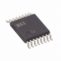
DS2764AE+ Maxim Integrated Products, DS2764AE+ Datasheet - Page 13

DS2764AE+
Manufacturer Part Number
DS2764AE+
Description
IC MON BATT LI-ION HP 16-TSSOP
Manufacturer
Maxim Integrated Products
Datasheet
1.DS2764AETR.pdf
(20 pages)
Specifications of DS2764AE+
Function
Battery Monitor
Battery Type
Lithium-Ion (Li-Ion)
Voltage - Supply
2.5 V ~ 5.5 V
Operating Temperature
-40°C ~ 85°C
Mounting Type
Surface Mount
Package / Case
16-TSSOP
Lead Free Status / RoHS Status
Lead free / RoHS Compliant
EEPROM to the shadow RAM. The Copy Data function command transfers data from the shadow RAM to the
EEPROM and requires t
POWER SWITCH INPUT
The DS2764 provides a power control function that uses the discharge protection FET to gate battery power to the
system. The PS pin, internally pulled to V
impedance connection to V
device to transition into active mode, turning on the discharge FET. If the DS2764 is already in active mode, activity
on PS has no effect on the FET control.
The host system has the option of monitoring activity on the PS pin by reading the PS bit in the Special Feature
Register. The PS bit latches a 0 value when a logic low occurs on the PS pin regardless of the operating mode of
the DS2764. If the host intends to monitor future PS pin events, it must write a 1 to the PS bit to ensure that a
subsequent low forced on the PS pin is latched into the PS bit. The PS bit value has no effect on operation of the
DS2764 and can be ignored if PS pin monitoring is not required.
MEMORY
The DS2764 has a 256-byte linear address space. Registers for instrumentation, status, and control are mapped
in the lower 32 bytes, with lockable EEPROM blocks and the unique ROM ID occupying portions of the remaining
address space. The Function Command Register occupies location FEh. All EEPROM memory is general purpose
except byte addresses 31h, 32h and 33h, which should be written with the default values for the Status register, 2-
Wire slave address and Current Offset register, respectively. When reading two-byte registers, (Current, ACR,
Voltage and Temperature), the MSB should be read first. When the MSB of two-byte registers is read, the MSB
and LSB are latched simultaneously and held for the duration of the Read Data transaction. This prevents register
updates during the read and ensures synchronization between the MSB and LSB of two byte register values. For
consistent results, always read the MSB and the LSB of a two-byte register during the same Read Data
transaction.
EEPROM memory is shadowed by RAM to eliminate programming delays between writes and to allow the data to
be verified by the host system before being copied to EEPROM. The Read Data and Write Data protocols to/from
EEPROM memory addresses access the shadow RAM. The Recall Data function command transfers data from the
data updates shadow RAM. In locked EEPROM blocks, attempts to write data are ignored. The Copy Data
function command copies the contents of shadow RAM to EEPROM in an unlocked block of EEPROM but has no
effect on locked blocks. The Recall Data function command copies the contents of a block of EEPROM to shadow
RAM regardless of whether the block is locked or not.
Figure 10. EEPROM Access via Shadow RAM
Interface
Serial
Read
EEC
SS
to complete programming of the EEPROM cells. In unlocked EEPROM blocks, writing
. If the DS2764 is in sleep mode, the detection of a low on the PS pin causes the
Write
DD
Shadow RAM
through a 1A current source, is continuously monitored for a low-
EEPROM
13 of 20
Recall
Copy


