MAX17006BETP+ Maxim Integrated Products, MAX17006BETP+ Datasheet - Page 13

MAX17006BETP+
Manufacturer Part Number
MAX17006BETP+
Description
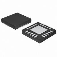
IC BATT CHARGER 1.2MHZ 20-TQFN
Manufacturer
Maxim Integrated Products
Specifications of MAX17006BETP+
Function
Charge Management
Battery Type
Multi-Chemistry
Voltage - Supply
8 V ~ 26 V
Operating Temperature
-40°C ~ 85°C
Mounting Type
Surface Mount
Package / Case
20-TQFN Exposed Pad
Lead Free Status / RoHS Status
Lead free / RoHS Compliant
Figure 4. Input Current-Limit Fine Tuning
The PWM filter accepts the digital signal with a frequency
from 128Hz to 500kHz. Zero duty cycle shuts down the
MAX17005/MAX17006/MAX17015, and 99.5% duty cycle
corresponds to full scale (60mV) across CSIP and CSIN.
Choose a current-sense resistor (RS2) to have a suffi-
cient power-dissipation rating to handle the full-charge
current. The current-sense voltage can be reduced to
minimize the power-dissipation period. However, this
can degrade accuracy due to the current-sense amplifi-
er’s input offset (0.25mV typ). See Typical Operating
Characteristics to estimate the charge-current accuracy
at various set points.
The total input current, from a wall adapter or other DC
source, is the sum of the system supply current and the
current required by the charger. When the input current
exceeds the set input-current limit, the controller
decreases the charge current to provide priority to sys-
tem load current. System current normally fluctuates as
portions of the system are powered up or down. The
input-current-limit circuit reduces the power require-
ment of the AC wall adapter, which reduces adapter
cost. As the system supply rises, the available charge
current drops linearly to zero. Thereafter, the total input
current can increase without limit.
The total input current is the sum of the device supply cur-
rent, the charger input current, and the system load cur-
rent. The total input current can be estimated as follows:
where η is the efficiency of the DC-to-DC converter
(typically 85% to 95%).
In the MAX17005/MAX17006/MAX17015, the voltage
across CSSP and CSSN is constant at 60mV. Choose
the current-sense resistor, RS1, to set the input current
limit. For example, for 4A input current limit, choose
RS1 = 15mΩ. For the input current-limit settings, which
cannot be achievable with standard sense resistor val-
ues, use a resistive voltage-divider between CSSP and
CSSN to tune the setting (Figure 4).
I
INPUT
MAX17005/MAX17006/MAX17015
=
I
LOAD
______________________________________________________________________________________
CSSP
Setting Input-Current Limit
+
RS1
Ra
I
CHARGE
CSSN
V
Rb
IN
×
× η
V
BATTERY
High-Performance Chargers
To minimize power dissipation, first choose RS1
according to the closest available value. For conve-
nience, choose Ra = 6kΩ and calculate Rb from the
above equation.
Choose a current-sense resistor (RS1) to have a suffi-
cient power rating to handle the full system current. The
current-sense resistor can be reduced to improve effi-
ciency, but this degrades accuracy due to the current-
sense amplifier’s input offset (0.15mV typ). See Typical
Operating Characteristics to estimate the input current-
limit accuracy at various set points.
The MAX17005/MAX17006/MAX17015 use an external
charge pump to drive the gate of an n-channel adapter
selection switch (N3 and Q1a). In Figure 1, when the
adapter is present, BST is biased 5V above V
so that N3 and Q1a are on, and Q1b is off. As long as
the adapter is present, even though the charger is off,
the power stage forces a refresh pulse to the BST
charge pump every 5ms.
When the adapter voltage is removed, the charger
stops generating BST refresh pulses and N4 forces N2
off, Q1b turns on and supplies power to the system
from the battery.
In Figure 1, D1 must have low forward-voltage drop and
low reverse-leakage current to ensure sufficient gate
drive at N3 and Q1a. A 100mA, low reverse-leakage
Schottky diode is the right choice.
Use IINP to monitor the system-input current, which is
sensed across CSSP and CSSN. The voltage at IINP is
proportional to the input current:
where I
adapter, G
amplifier (2.8 mA/V typ), and R
nected between IINP and ground. Typically, IINP has a
0V to 3.5V output voltage range. Leave IINP unconnect-
ed when not used.
INPUT
Analog Input Current-Monitor Output
Automatic Power-Source Selection
IINP
1.2MHz Low-Cost,
I
INPUT LIMIT
I
INPUT
is the DC current supplied by the AC
is the transconductance of the sense
_
=
RS
1
=
×
60
G
RS
V
IINP
mV
IINP
1
IINP
× +
×
(
R
1
is the resistor con-
IINP
Rb
Ra
)
ADAPTER
13


