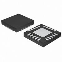
MAX17006BETP+ Maxim Integrated Products, MAX17006BETP+ Datasheet - Page 18

MAX17006BETP+
Manufacturer Part Number
MAX17006BETP+
Description
IC BATT CHARGER 1.2MHZ 20-TQFN
Manufacturer
Maxim Integrated Products
Specifications of MAX17006BETP+
Function
Charge Management
Battery Type
Multi-Chemistry
Voltage - Supply
8 V ~ 26 V
Operating Temperature
-40°C ~ 85°C
Mounting Type
Surface Mount
Package / Case
20-TQFN Exposed Pad
Lead Free Status / RoHS Status
Lead free / RoHS Compliant
If R
a negligible effect near crossover and the loop-transfer-
function can be simplified as follows:
Setting LTF = 1 to solve for the unity-gain frequency
yields:
For stability, choose a crossover frequency lower than
1/10 the switching frequency (f
choose a crossover frequency of 50kHz and solve for
R
yield R
GMV = 0.125μA/mV
GM
C
f
R
f
To ensure that the compensation zero adequately can-
cels the output pole, select f
C
charge current).
Figure 8. CC Loop Response
1.2MHz Low-Cost,
High-Performance Chargers
18
OSC_CV
CO_CV
CC
L
OUT
CC
= 0.2Ω
ESR
OUT
______________________________________________________________________________________
using the component values listed in Figure 1 to
≥ 300pF (assuming 2 cells and 2A maximum
= 4.7μF
CC
= 50kHz
is small enough, its associated output zero has
= 5A/V
f
= 600kHz
-20
-40
CO CV
80
60
40
20
= 3kΩ:
0
R
0.1
_
CC
LTF
=
C
1
=
CC
2
=
GM
MAG
PHASE
π
GM
10
GMV GM
≥ (R
×
OUT
FREQUENCY (Hz)
C
OUT
OUT
100
L
×
/R
×
×
Z_CV
CC
G
×
1k
sC
MV
f
CO CV
) x C
R
OUT
CC
OUT
10k
≤ f
×
_
OSC)
2π
OUT
P_OUT
G
100k
R
×
MV
≅
CC
. For example,
C
3
OUT
k
1M
:
Ω
0
-45
-90
-135
Figure 8 shows the Bode plot of the voltage-loop-
frequency response using the values calculated above.
The DHI and DLO outputs are optimized for driving
moderate-sized power MOSFETs. The MOSFET drive
capability is the same for both the low-side and high-
sides switches. This is consistent with the variable duty
factor that occurs in the notebook computer environ-
ment where the battery voltage changes over a wide
range. There must be a low-resistance, low-inductance
path from the DLO driver to the MOSFET gate to pre-
vent shoot-through. Otherwise, the sense circuitry in the
MAX17005/MAX17006 interpret the MOSFET gate as
“off” while there is still charge left on the gate. Use very
short, wide traces measuring 10 to 20 squares or fewer
(1.25mm to 2.5mm wide if the MOSFET is 25mm from
the device). Unlike the DLO output, the DHI output uses
a 50ns (typ) delay time to prevent the low-side MOSFET
from turning on until DHI is fully off. The same consider-
ations should be used for routing the DHI signal to the
high-side MOSFET.
The high-side driver (DHI) swings from LX to 5V above
LX (BST) and has a typical impedance of 1.5Ω sourcing
and 0.8Ω sinking. The strong high-side MOSFET driver
eliminates most of the power dissipation due to switch-
ing losses. The low-side driver (DLO) swings from LDO
to ground and has a typical impedance of 3Ω sinking
and 3Ω sourcing. This helps prevent DLO from being
pulled up when the high-side switch turns on due to
capacitive coupling from the drain to the gate of the
low-side MOSFET. This places some restrictions on the
MOSFETs that can be used. Using a low-side
MOSFET with smaller gate-to-drain capacitance can
prevent these problems.
Choose the n-channel MOSFETs according to the maxi-
mum required charge current. The MOSFETs must be
able to dissipate the resistive losses plus the switching
losses at both V
For the high-side MOSFET, the worst-case resistive
power losses occur at the maximum battery voltage
and minimum supply voltage:
PD
COND
(
HighSide
DCIN(MIN)
)
=
V
V
BATT MAX
DCIN MIN
and V
Design Procedure
(
(
MOSFET Selection
DCIN(MAX)
)
)
MOSFET Drivers
×
I
CHG
2
.
× × R
DS ON
(
)


