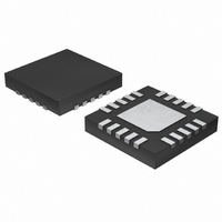
MAX17006BETP+ Maxim Integrated Products, MAX17006BETP+ Datasheet - Page 19

MAX17006BETP+
Manufacturer Part Number
MAX17006BETP+
Description
IC BATT CHARGER 1.2MHZ 20-TQFN
Manufacturer
Maxim Integrated Products
Specifications of MAX17006BETP+
Function
Charge Management
Battery Type
Multi-Chemistry
Voltage - Supply
8 V ~ 26 V
Operating Temperature
-40°C ~ 85°C
Mounting Type
Surface Mount
Package / Case
20-TQFN Exposed Pad
Lead Free Status / RoHS Status
Lead free / RoHS Compliant
Generally, a low gate charge high-side MOSFET is pre-
ferred to minimize switching losses. However, the
R
pation often limits how small the MOSFET can be. The
optimum occurs when the switching losses equal the
conduction losses. High-side switching losses do not
usually become an issue until the input is greater than
approximately 15V. Calculating the power dissipation in
N1 due to switching losses is difficult since it must
allow for difficult quantifying factors that influence the
turn-on and turn-off times. These factors include the
internal gate resistance, gate charge, threshold volt-
age, source inductance, and PCB layout characteris-
tics. The following switching-loss calculation provides
only a very rough estimate and is no substitute for
breadboard evaluation, preferably including a verifica-
tion using a thermocouple mounted on N1:
where t
calculated as follows:
I
current (3Ω sourcing and 0.8Ω sinking, typically). The
MAX17005/MAX17006/MAX17015 control the switching
frequency as shown in the Typical Operating
Characteristics .
The following is the power dissipated due to high-side
n-channel MOSFET’s output capacitance (C
The following high-side MOSFET’s loss is due to the
reverse-recovery charge of the low-side MOSFET’s
body diode:
Ignore PD
parallel to a low-side MOSFET.
The total high-side MOSFET power dissipation is:
GSRC
DS(ON)
PD
and I
t
TRANS
TRANS
PD
SW
required to stay within package power dissi-
PD
QRR
PD
TOTAL
(
GSNK
HS
CRSS
QRR
is the drivers transition time and can be
(HighSide) if a Schottky diode is used
=
) =
⎛
⎝ ⎜
(
(
HS
I
(
GSRC
HS
______________________________________________________________________________________
HS
1
2
are the peak gate-drive source/sink
×
1
)
) ≈
) =
+
≈
t
TRANS
PD
PD
+
V
Q
2
I
RR
COND
GSNK
CRSS
CSSP
1
2
×
×
V
(
(
HS
⎞
⎠ ⎟
×
V
CSSP
HS
CSSP
2
×
C
2
)
(
RSS
)
+
Q
+
PD
GD
×
PD
×
I
×
CHG
QRR
f
SW
SW
+
f
SW
Q
RSS
(
HS
×
(
GS
HS
f
SW
)
):
)
)
High-Performance Chargers
Switching losses in the high-side MOSFET can become
an insidious heat problem when maximum AC adapter
voltages are applied. If the high-side MOSFET chosen
for adequate R
hot when biased from V
another MOSFET with lower parasitic capacitance.
For the low-side MOSFET (N2), the worst-case power
dissipation always occurs at maximum input voltage:
The following additional loss occurs in the low-side
MOSFET due to the body diode conduction losses:
The total power low-side MOSFET dissipation is:
These calculations provide an estimate and are not a
substitute for breadboard evaluation, preferably
including a verification using a thermocouple mounted
on the MOSFET.
The selection of the inductor has multiple trade-offs
between efficiency, transient response, size, and cost.
Small inductance is cheap and small, and has a better
transient response due to higher slew rate; however, the
efficiency is lower because of higher RMS current. High
inductance results in lower ripple so that the need of the
output capacitors for output voltage ripple goes low.
The MAX17005/MAX17006/MAX17015 combine all the
inductor trade-offs in an optimum way by controlling
switching frequency. High-frequency operation permits
the use of a smaller and cheaper inductor, and conse-
quently results in smaller output ripple and better tran-
sient response.
The charge current, ripple, and operating frequency
(off-time) determine the inductor characteristics. For
optimum efficiency, choose the inductance according
to the following equation:
where k = 35ns/V.
PD
COND
PD
TOTAL
( )
1.2MHz Low-Cost,
PD
LS
BDY
DS(ON)
=
( )
L
LS
⎛
⎜
⎝
=
( )
1
LS
−
4
≈
V
at low-battery voltages becomes
×
V
PD
=
CSSP MAX
BATT MIN
I
CHG
DCIN(MAX)
0 05
COND
k V
.
×
(
(
×
×
IN
LIR
( )
I
Inductor Selection
PEAK
LS
2
)
)
⎞
⎟ ×
⎠
MAX
, consider choosing
+
I
PD
×
CH
0 4
BDY
G G
.
2
V
×
( )
LS
R
DS ON
(
)
19


