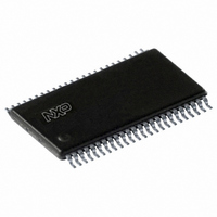
PCF8562TT/2,118 NXP Semiconductors, PCF8562TT/2,118 Datasheet - Page 17

PCF8562TT/2,118
Manufacturer Part Number
PCF8562TT/2,118
Description
IC LCD DRIVER 32/128SEG 48-TSSOP
Manufacturer
NXP Semiconductors
Datasheet
1.PCF8562TT2118.pdf
(37 pages)
Specifications of PCF8562TT/2,118
Package / Case
48-TSSOP
Display Type
LCD
Configuration
7 Segment + DP, 14 Segment (32 Segment)
Interface
I²C
Current - Supply
32µA
Voltage - Supply
1.8 V ~ 5.5 V
Operating Temperature
-40°C ~ 85°C
Mounting Type
Surface Mount
Number Of Digits
16
Number Of Segments
32
Maximum Clock Frequency
2640 Hz
Operating Supply Voltage
1.8 V to 5.5 V
Maximum Power Dissipation
400 mW
Maximum Operating Temperature
+ 85 C
Attached Touch Screen
No
Maximum Supply Current
20 uA
Minimum Operating Temperature
- 40 C
Lead Free Status / RoHS Status
Lead free / RoHS Compliant
For Use With
OM6292 - DEMO BOARD PCA2125 RTCOM10088 - KIT FOR LCD DEMO LPC900622-1003 - KIT FOR LCD DEMO
Digits Or Characters
-
Lead Free Status / Rohs Status
Lead free / RoHS Compliant
Other names
568-2029-2
PCF8562TT/2,518
PCF8562TT/2-T
PCF8562TT/2,518
PCF8562TT/2-T
NXP Semiconductors
PCF8562_5
Product data sheet
7.12 Subaddress counter
7.13 Output bank selector
7.11 Data pointer
The addressing mechanism for the display RAM is realized using the data pointer.
This allows the loading of an individual display data byte, or a series of display data bytes,
into any location of the display RAM. The sequence commences with the initialization of
the data pointer by the load-data-pointer command (see
Following this command, an arriving data byte is stored at the display RAM address
indicated by the data pointer. The filling order shown in
After each byte is stored, the contents of the data pointer is automatically incremented by
a value dependent on the selected LCD drive mode:
If an I
The data pointer should be re-written prior to further RAM accesses.
The storage of display data is determined by the contents of the subaddress counter.
Storage is allowed to take place only when the contents of the subaddress counter agree
with the hardware subaddress applied to A0, A1 and A2. The subaddress counter value is
defined by the device-select command (see
subaddress counter and the hardware subaddress do not agree then data storage is
inhibited but the data pointer is incremented as if data storage had taken place. The
subaddress counter is also incremented when the data pointer overflows.
The hardware subaddress must not be changed while the device is being accessed on the
I
The output bank selector selects one of the four rows per display RAM address for
transfer to the display register. The actual row selected depends on the particular LCD
drive mode in operation and on the instant in the multiplex sequence.
The PCF8562 includes a RAM bank switching feature in the static and 1:2 drive modes. In
the static drive mode, the bank-select command (see
contents of row 2 to be selected for display instead of the contents of row 0. In 1:2 mode,
2
•
•
•
•
C-bus interface.
•
•
•
•
In static drive mode by eight
In 1:2 multiplex drive mode by four
In 1:3 multiplex drive mode by three
In 1:4 multiplex drive mode by two
In 1:4 multiplex mode, all RAM addresses of row 0 are selected, these are followed by
the contents of row 1, row 2 and then row 3.
In 1:3 multiplex mode, row 0, 1 and 2 are selected sequentially
In 1:2 multiplex mode, row 0 and 1 are selected
In static mode, row 0 is selected
2
C-bus data access is terminated early then the state of the data pointer is unknown.
All information provided in this document is subject to legal disclaimers.
Rev. 05 — 19 May 2010
Universal LCD driver for low multiplex rates
Section
7.17). If the contents of the
Section
Figure
Section
7.17) may request the
10.
7.17).
PCF8562
© NXP B.V. 2010. All rights reserved.
17 of 37


