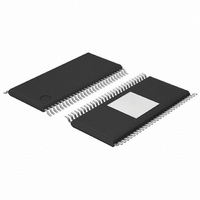
PCF8576CTT/1,118 NXP Semiconductors, PCF8576CTT/1,118 Datasheet - Page 24

PCF8576CTT/1,118
Manufacturer Part Number
PCF8576CTT/1,118
Description
IC LCD DVR UNIVERSAL 56-HTSSOP
Manufacturer
NXP Semiconductors
Datasheet
1.PCF8576CTT1118.pdf
(57 pages)
Specifications of PCF8576CTT/1,118
Package / Case
56-TSSOP Exposed Pad, 56-eTSSOP, 56-HTSSOP
Display Type
LCD
Configuration
40 Segment
Interface
I²C
Current - Supply
120µA
Voltage - Supply
2 V ~ 6 V
Operating Temperature
-40°C ~ 85°C
Mounting Type
Surface Mount
Number Of Digits
20
Number Of Segments
160
Maximum Clock Frequency
315 KHz
Operating Supply Voltage
2 V to 6 V
Maximum Power Dissipation
400 mW
Maximum Supply Current
120 uA
Lead Free Status / RoHS Status
Lead free / RoHS Compliant
Digits Or Characters
-
Lead Free Status / Rohs Status
Lead free / RoHS Compliant
Other names
935284868118
PCF8576CTT/1-T
PCF8576CTT/1-T
PCF8576CTT/1-T
PCF8576CTT/1-T
NXP Semiconductors
PCF8576C
Product data sheet
7.16.1 Bit transfer
7.16.2 START and STOP conditions
7.16 Characteristics of the I
In the 1:3 and 1:4 multiplex modes, where no alternate RAM bank is available, groups of
LCD segments can be blinked by selectively changing the display RAM data at fixed time
intervals.
If the entire display needs to be blinked at a frequency other than the nominal blink
frequency, this can be done using the mode-set command to set and reset the display
enable bit E at the required rate (see
The I
The two lines are a Serial DAta line (SDA) and a Serial Clock Line (SCL). Both lines must
be connected to a positive supply via a pull-up resistor when connected to the output
stages of a device. Data transfer may be initiated only when the bus is not busy.
One data bit is transferred during each clock pulse. The data on the SDA line must remain
stable during the HIGH period of the clock pulse. Changes in the data line at this time will
be interpreted as a control signal. Bit transfer is illustrated in
Both data and clock lines remain HIGH when the bus is not busy. A HIGH-to-LOW change
of the data line, while the clock is HIGH, is defined as the START condition (S).
A LOW-to-HIGH change of the data line, while the clock is HIGH, is defined as the STOP
condition (P). The START and STOP conditions are illustrated in
Fig 15. Bit transfer
Fig 16. Definition of START and STOP conditions
2
C-bus is for bidirectional, two-line communication between different ICs or modules.
SDA
SCL
START condition
All information provided in this document is subject to legal disclaimers.
SDA
SCL
S
Rev. 10 — 22 July 2010
2
C-bus
data valid
data line
stable;
Table
Universal LCD driver for low multiplex rates
9).
allowed
change
of data
Figure
STOP condition
Figure
mba607
PCF8576C
P
15.
© NXP B.V. 2010. All rights reserved.
16.
mbc622
SDA
SCL
24 of 57


