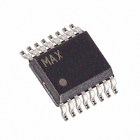
MAX6852AEE+T Maxim Integrated Products, MAX6852AEE+T Datasheet - Page 15

MAX6852AEE+T
Manufacturer Part Number
MAX6852AEE+T
Description
IC VFD CTRLR MATRIX 16QSOP
Manufacturer
Maxim Integrated Products
Datasheet
1.MAX6852AEET.pdf
(32 pages)
Specifications of MAX6852AEE+T
Display Type
Vacuum Fluorescent (VF)
Configuration
5 x 7 (Matrix)
Interface
Serial
Current - Supply
3.5mA
Voltage - Supply
2.7 V ~ 3.6 V
Operating Temperature
-40°C ~ 125°C
Mounting Type
Surface Mount
Package / Case
16-QSOP
Lead Free Status / RoHS Status
Lead free / RoHS Compliant
Digits Or Characters
-
ister, high-voltage grid/anode VFD tube drivers (Figures
3 and 4). The speed of VFCLK is 2MHz when OSC is
4MHz. The maximum speed of VFCLK is 4MHz when
OSC is 8MHz. This interface is used to transfer display
data from the MAX6852 to the VFD tube driver. The ser-
ial interface bit stream output is programmable up to
122 bits, which are labeled DD0–DD121.
The functions of the three interface pins are as follows:
VFCLK is the serial clock output, which shifts data on
its falling edge from the MAX6852’s 122-bit output shift
register to VFLOAD.
VFDOUT is the serial data output. The data changes on
VFCLK’s falling edge, and is stable when it is sampled
by the display driver on the rising edge of VFCLK.
VFLOAD is the latch-load output. VFLOAD is high to
transfer data from the display tube driver’s shift register to
the display driver’s output latch (transparent mode), and
low to retain that data in the display driver’s output latch.
A fourth output pin, VFBLANK, provides gating control
of the tube driver. VFBLANK can be configured to be
either high or low using the VBLANK polarity register
(Table 26) to enable the VFD tube driver. In the default
condition, VFBLANK is high to disable the VFD tube dri-
ver, which is expected to force its driver outputs low to
blank the display without altering the contents of its out-
put latches. In the default condition, VFBLANK is low to
enable its VFD tube driver outputs to follow the state of
the VFD tube driver’s output latches. The VFBLANK
output is used for PWM intensity control and to disable
the VFD tube driver in shutdown.
The multiplex engine transmits grid and anode control
data to the external VFD driver using the VFCLK, VFD-
OUT, and VFLOAD. The number of data bits m trans-
mitted is set by the user in the shift-limit register (Table
28). Figure 10 is the VFD multiplex timing diagram.
Figure 8. Transmission of More than 16 Bits to the MAX6852
DOUT
CLK
DIN
CS
BIT
1
______________________________________________________________________________________
BIT
2
4-Wire Interfaced, 5
N-15
= 0
N-31
Multiplex Architecture
N-14
N-30
N-13
N-29
N-12
N-28
Fluorescent Display Controller
N-11
N-27
N-10
N-26
N-9
N-25
The essential rules for multiplex action are as follows:
• The external VFD driver’s data latch contains the
• The VFBLANK input is controlled to provide the
• The VFCLK and VFDOUT outputs are used to fill the
• The VFLOAD output loads the new grid-anode data
The grids register sets how many grids are multiplexed
from 1 to 48 (Table 24).
When the grids register is written, the external VFD tube
driver is presumed to contain invalid data. The
VFBLANK output is used to disable the VFD tube driver
for the first multiplex cycle after exiting shutdown, clear-
ing any invalid data. The next multiplex cycle uses
newly sent, valid data. If the grids register is written
with an out-of-range value of 0x30 to 0xFF, then the
value 0x2F is stored instead.
Digital control of display brightness is provided by
pulse-width modulation of the tube blanking time, which
is controlled by the lower nibble of the intensity register
(Table 25). The modulator scales the VFBLANK output
in 15 steps from a minimum of 1/16 up to 15/16 of each
grid’s multiplex period (Figure 11). Figure 12 shows the
modulator behavior when the VFBLANK polarity regis-
ter is set to 0x00 (Table 26), so VFBLANK is high to dis-
able (blank) the display.
The minimum off-time period of a 1/16 multiplex period
(6.25µs with OSC = 4MHz) is always at the start of the
multiplex cycle. This allows time for slow display drivers
to turn off, and slow display phosphors time to decay
N-8
N-24
data for the current grid being displayed.
PWM intensity control.
external VFD driver’s shift register with the multiplex
data for the next grid, during the multiplex timeslot
for the current grid.
pattern at the start of its multiplex cycle.
N-7
N-23
✕
N-22
N-6
7 Matrix Vacuum-
N-21
N-5
N-20
N-4
N-19
N-3
N-18
Intensity Register
N-2
Grids Register
N-17
N-1
N-16
N
N-15 = 0
15


