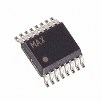
MAX6852AEE+T Maxim Integrated Products, MAX6852AEE+T Datasheet - Page 16

MAX6852AEE+T
Manufacturer Part Number
MAX6852AEE+T
Description
IC VFD CTRLR MATRIX 16QSOP
Manufacturer
Maxim Integrated Products
Datasheet
1.MAX6852AEET.pdf
(32 pages)
Specifications of MAX6852AEE+T
Display Type
Vacuum Fluorescent (VF)
Configuration
5 x 7 (Matrix)
Interface
Serial
Current - Supply
3.5mA
Voltage - Supply
2.7 V ~ 3.6 V
Operating Temperature
-40°C ~ 125°C
Mounting Type
Surface Mount
Package / Case
16-QSOP
Lead Free Status / RoHS Status
Lead free / RoHS Compliant
Digits Or Characters
-
4-Wire Interfaced, 5
Fluorescent Display Controller
Figure 9. VFD Interface Timing Diagram
Figure 10. VFD Multiplex Timing Diagram
between grids. Thus, image ghosting is avoided. If a
display has very slow phosphor, then the allowed decay
time can be doubled by not using a 15/16 duty cycle.
The VFBLANK polarity register sets the active level of
the VFBLANK output pin (Table 26).
A write to the no-op register is ignored.
Writing the display-test and device ID register switches
the drivers between one of two modes: normal and dis-
play test. Display-test mode turns all segments and
annunciators on and sets the duty cycle to 7/16 (half-
power) (Table 27).
16
VFDOUT
VFLOAD
VFCLK
______________________________________________________________________________________
VFLOAD
VFDOUT
VFCLK
Display-Test and Device ID Register
500ns
100µs TIMESLOT
500ns
GRID 0
500ns 500ns
DD0 DD1 DD2 DD3
VFBLANK Polarity Register
100µs TIMESLOT
GRID 1
DD4 DD5 DD6 DD7 DD8 DD9 DD10
GRID 1's DATA, SENT DURING GRID 0's TIMESLOT
ONE COMPLETE MULTIPLEX CYCLE AROUND N GRIDS (OSC = 4MHz)
No-Op Register
t
VDS
DD0
100µs TIMESLOT
GRID N-4
t
VCL
GRID 0's 100µs MULTIPLEX TIMESLOT
✕
DD1
7 Matrix Vacuum-
t
VCH
100µs TIMESLOT
GRID N-3
Reading the display-test and device ID register returns
the MAX6852 device ID 0b0000 011 that identifies the
driver type, plus the display-test status in the LSB.
The output serial interface is used to transfer display
data from the MAX6852 to the display driver. The serial
interface bit-stream output length is programmable up
to 122 bits, which are labeled DD0–DD121. Set the
number of bits with the shift-limit register, address
0x0E. If the shift-limit register is written with an out-of-
range value 0x7A to 0xFF, then the value 0x79 is stored
instead. Table 28 shows the shift-limit register.
The output map comprises 122 words of 7-bit RAM.
The output map data should be written when the
MAX6852 is configured after power-up. Table 29 shows
the output map RAM codes.
M-4
M-3
100µs TIMESLOT
M-1
M-2 M-1
GRID N-2
t
VCP
M
Output Shift-Limit Register
M (M IS VALUE IN SHIFT-LIMIT REGISTER)
(M IS VALUE IN SHIFT-LIMIT REGISTER)
100µs TIMESLOT
t
GRID N-1
VCSH
t
VCSW
100µs TIMESLOT
GRID 0
Output Map
START OF NEXT
CYCLE


