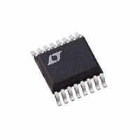
LTC1647-3CGN#PBF Linear Technology, LTC1647-3CGN#PBF Datasheet - Page 13

LTC1647-3CGN#PBF
Manufacturer Part Number
LTC1647-3CGN#PBF
Description
IC CTLR HOTSWAP DUAL 16-SSOP
Manufacturer
Linear Technology
Type
Hot-Swap Controllerr
Specifications of LTC1647-3CGN#PBF
Applications
General Purpose
Internal Switch(s)
No
Voltage - Supply
2.7 V ~ 16.5 V
Operating Temperature
0°C ~ 70°C
Mounting Type
Surface Mount
Package / Case
16-SSOP (0.150", 3.90mm Width)
Linear Misc Type
Positive Low Voltage
Family Name
LTC1647-3
Package Type
SSOP N
Operating Supply Voltage (min)
2.7V
Operating Supply Voltage (max)
16.5V
Operating Temperature (min)
0C
Operating Temperature (max)
70C
Operating Temperature Classification
Commercial
Product Depth (mm)
3.99mm
Product Height (mm)
1.5mm
Mounting
Surface Mount
Pin Count
16
Lead Free Status / RoHS Status
Lead free / RoHS Compliant
Available stocks
Company
Part Number
Manufacturer
Quantity
Price
APPLICATIO S I FOR ATIO
If a dead short occurs after a supply connection is made
(Figure 12), the sense resistor R1 and the R
enhanced Q1 provide a low impedance path for nearly
unlimited current flow. The LTC1647 discharges the GATE
pin in a few microseconds, but during this discharge time
current on the order of 150 amperes flows from the V
power supply. This current spike glitches the power sup-
ply, causing V
On recovery from overload, some supplies may over-
shoot. Other devices attached to this supply may reset or
malfunction and the overshoot may also damage some
components. An inductor (1 H to 10 H) in series with
Q1’s source limits the short-circuit di/dt, thereby limiting
the peak current and the supply glitch (Figure 12c and
12d). Additional power supply bypass capacitance also
reduces the magnitude of the V
CC
to dip (Figure 12a and 12b).
U
U
CC
glitch.
W
DS(ON)
U
of fully
CC
LTC1647-1/LTC1647-2/LTC1647-3
V
The two Hot Swap channels of the LTC1647 are ideally
suited for V
Figure 13 shows an application using the LTC1647-2 on
the system side of the device bay interface (1394 PHY and/
or USB). The controller detects the presence of a periph-
eral in each device bay and controls the LTC1647-2. The
timing waveform illustrates the following sequence of
events: t1, rising out of undervoltage lockout with GATE 1
ramping up; t2, load current fault at R1; t3, circuit breaker
resets with R5/C3 delay; t4/t5, controller gates off/on
device supply with RC delay; t6, device enters undervolt-
age lockout.
If C6 is not connected in Figure 13, FAULT 2 and ON2 will
have similar waveforms. t7 initiates an ON sequence; t8, a
load fault is detected at R7 with FAULT 2 pulling low. If the
controller wants to stretch the interval between retries, it
can pull ON2 low at t9 ( t9 – t8 < 0.4•t
controller initiates a new power-up/down sequence.
ID
Power Controller
ID
power control in portable computers.
RESET
). At t10/t11, the
13


