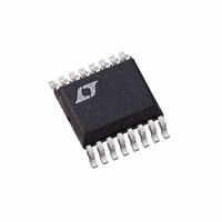
LTC1647-3CGN#PBF Linear Technology, LTC1647-3CGN#PBF Datasheet - Page 9

LTC1647-3CGN#PBF
Manufacturer Part Number
LTC1647-3CGN#PBF
Description
IC CTLR HOTSWAP DUAL 16-SSOP
Manufacturer
Linear Technology
Type
Hot-Swap Controllerr
Specifications of LTC1647-3CGN#PBF
Applications
General Purpose
Internal Switch(s)
No
Voltage - Supply
2.7 V ~ 16.5 V
Operating Temperature
0°C ~ 70°C
Mounting Type
Surface Mount
Package / Case
16-SSOP (0.150", 3.90mm Width)
Linear Misc Type
Positive Low Voltage
Family Name
LTC1647-3
Package Type
SSOP N
Operating Supply Voltage (min)
2.7V
Operating Supply Voltage (max)
16.5V
Operating Temperature (min)
0C
Operating Temperature (max)
70C
Operating Temperature Classification
Commercial
Product Depth (mm)
3.99mm
Product Height (mm)
1.5mm
Mounting
Surface Mount
Pin Count
16
Lead Free Status / RoHS Status
Lead free / RoHS Compliant
Available stocks
Company
Part Number
Manufacturer
Quantity
Price
BLOCK DIAGRA S
APPLICATIO S I FOR ATIO
V
The LTC1647-3 features separate supply inputs (V
V
circuit draw supply current from the higher of the two
supplies. An internal V
makes the power connection automatically. This allows a
3V channel to have standard MOSFET gate overdrive when
the other channel is 5V. An internal Zener clamps GATE
about 15V above V
If both supplies are connected together (internally for
LTC1647-1 and LTC1647-2 or externally for LTC1647-3),
the reference and charge pump circuit draw equal current
from both pins.
Electronic Circuit Breaker
Each channel of the LTC1647 features an electronic circuit
breaker to protect against excessive load current and
CC
CC2
Selection Circuit
) for each channel. The reference and charge pump
SENSE 1
SENSE 2
FAULT 1
FAULT 2
V
V
GND
ON1
ON2
CC1
CC2
CC
U
16
15
14
1
8
2
3
4
5
.
CC
U
W
selection circuit detects and
+
–
1.21V
50mV
W
REFERENCE
+
–
+
–
2.45V
UVL
1.21V
U
CC1
FILTER
50 s
(DUPLICATE OF CHANNEL ONE)
and
CHARGE
PUMP
LTC1647-3
CHANNEL TWO
CHANNEL ONE
LTC1647-1/LTC1647-2/LTC1647-3
FAULT
short-circuits. Load current is monitored by sense resis-
tor R1 as shown in Figure 1. The circuit breaker threshold,
V
approximately 300ns. If the voltage between V
SENSE exceeds V
breaker trips and immediately pulls GATE low with a 50mA
current sink. The MOSFET turns off and FAULT pulls low.
The circuit breaker is cleared by pulling the ON pin low for
a period of at least t
events is shown in Figure 2.
The value of the sense resistor R1 is given by
where V
I
breaker trips. Kelvin-sense layout techniques between the
sense resistor and the V
recommended for proper operation.
CP
TRIP
CB
R1 = V
, is 50mV and it exhibits a response time, t
is the value of the load current at which the circuit
SELECTION
CB
V
CC
CB
is the circuit breaker trip voltage (50mV) and
/I
TRIP
( )
RESET
CB
CP
for more than t
10 A
50 A
(50 s). A timing diagram of these
CC
and SENSE pins are highly
1647-1/2/3 BD3
13
12
FAULT
GATE 1
GATE 2
, the circuit
FAULT
CC
9
and
, of


