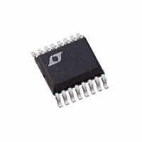
LTC1647-3CGN#PBF Linear Technology, LTC1647-3CGN#PBF Datasheet - Page 7

LTC1647-3CGN#PBF
Manufacturer Part Number
LTC1647-3CGN#PBF
Description
IC CTLR HOTSWAP DUAL 16-SSOP
Manufacturer
Linear Technology
Type
Hot-Swap Controllerr
Specifications of LTC1647-3CGN#PBF
Applications
General Purpose
Internal Switch(s)
No
Voltage - Supply
2.7 V ~ 16.5 V
Operating Temperature
0°C ~ 70°C
Mounting Type
Surface Mount
Package / Case
16-SSOP (0.150", 3.90mm Width)
Linear Misc Type
Positive Low Voltage
Family Name
LTC1647-3
Package Type
SSOP N
Operating Supply Voltage (min)
2.7V
Operating Supply Voltage (max)
16.5V
Operating Temperature (min)
0C
Operating Temperature (max)
70C
Operating Temperature Classification
Commercial
Product Depth (mm)
3.99mm
Product Height (mm)
1.5mm
Mounting
Surface Mount
Pin Count
16
Lead Free Status / RoHS Status
Lead free / RoHS Compliant
Available stocks
Company
Part Number
Manufacturer
Quantity
Price
PI FU CTIO S
V
supply range for normal operation is 2.7V to 16.5V. The
supply current, I
voltage lockout (UVLO) circuit disables GATE 1 until the
supply voltage at V
2.45V). GATE 1 is held at ground potential until UVLO
deactivates. If ON1 is high and V
threshold voltage, GATE 1 is pulled high by a 10 A current
source. If V
immediately to ground. The internal reference and the
common charge pump are powered from the higher of the
two V
V
V
V
and the LTC1647-2. V
nected together.
GND: Chip Ground.
ON1: Channel 1 ON Input. The threshold at the ON1 pin is
set at 1.29V with 70mV hysteresis. If UVLO and the circuit
breaker of channel 1 are inactive, a logic high at ON1
enables the 10 A charge pump current source, pulling the
GATE 1 pin above V
GATE 1 pin is pulled to ground by a 50 A current sink.
ON1 resets channel 1’s electronic circuit breaker by pull-
ing ON1 low for greater than one t
low-to-high transition at ON1 restarts a normal GATE 1
pull-up sequence.
ON2: Channel 2 ON Input. See ON1 for functional descrip-
tion.
CC1
CC2
CC1
CC
U
: The Common Positive Supply Input for the LTC1647-1
(LTC1647-3): Channel 1 Positive Supply Input. The
(LTC1647-3): Channel 2 Positive Supply Input. See
for functional description.
CC
inputs, V
U
CC1
falls below (V
CC1
CC1
, is typically 1mA. Channel 1’s under-
CC1
CC1
U
or V
CC1
. If the ON1 pin is pulled low, the
is greater than V
CC2
and V
LKO
.
– V
CC2
CC1
RESET
LKH
is above the UVLO
are internally con-
), GATE 1 is pulled
period (50 s). A
LKO
(typically
LTC1647-1/LTC1647-2/LTC1647-3
FAULT 1: Channel 1 Open-Drain Fault Status Output.
FAULT 1 pin pulls low after 0.3 s (t
breaker measures greater than 50mV across the sense
resistor connected between V
pulls low, GATE 1 also pulls low. FAULT 1 remains low until
ON1 is pulled low for at least one t
FAULT 2: Channel 2 Open-Drain Fault Status Output. See
FAULT 1 for functional description.
SENSE 1: Channel 1 Circuit Breaker Current Sense Input.
Load current is monitored by a sense resistor connected
between V
voltage across the sense resistor exceeds 50mV (V
disable the circuit breaker, connect SENSE 1 to V
order to obtain optimum performance, use Kelvin-sense
connections between the V
current sense resistor.
SENSE 2: Channel 2 Circuit Breaker Current Sense Input.
See SENSE 1 for functional description.
GATE 1: Channel 1 N-Channel MOSFET Gate Drive Output.
An internal charge pump guarantees at least 10V of gate
drive from a 5V supply. Two Zener clamps are incorpo-
rated at the GATE 1 pin; one Zener clamps GATE 1
approximately 15V above V
clamps GATE 1 appoximately 28V above GND. The rise
time at GATE 1 is set by an external capacitor connected
between GATE 1 and GND and an internal 10 A current
source provided by the charge pump. The fall time at GATE
1 is set by the 50 A current sink if ON1 is pulled low. If the
circuit breaker is tripped or the supply voltage hits the
UVLO threshold, a 50mA current sink rapidly pulls GATE 1
low.
GATE 2: Channel 2 N-Channel MOSFET Gate Drive Output.
See GATE 1 for functional description.
NC: No Connection.
CC1
and SENSE 1. The circuit breaker trips if the
CC
CC1
CC
and SENSE pins to the
and SENSE 1. If FAULT 1
and the second Zener
RESET
FAULT
period.
) if the circuit
CB
CC1
). To
7
. In


