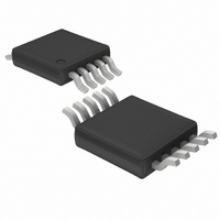
LTC4214-1CMS#PBF Linear Technology, LTC4214-1CMS#PBF Datasheet - Page 11

LTC4214-1CMS#PBF
Manufacturer Part Number
LTC4214-1CMS#PBF
Description
IC CTRLR HOTSWAP NEGVOLT 10MSOP
Manufacturer
Linear Technology
Type
Hot-Swap Controllerr
Datasheet
1.LTC4214-1CMS.pdf
(32 pages)
Specifications of LTC4214-1CMS#PBF
Applications
General Purpose
Internal Switch(s)
No
Voltage - Supply
6 V ~ 16 V
Operating Temperature
0°C ~ 70°C
Mounting Type
Surface Mount
Package / Case
10-TFSOP, 10-MSOP (0.118", 3.00mm Width)
Linear Misc Type
Negative Low Voltage
Family Name
LTC4214-1
Package Type
MSOP
Operating Supply Voltage (min)
-6V
Operating Supply Voltage (max)
-16V
Operating Temperature (min)
0C
Operating Temperature (max)
70C
Operating Temperature Classification
Commercial
Product Depth (mm)
3mm
Product Height (mm)
0.86mm
Product Length (mm)
3mm
Mounting
Surface Mount
Pin Count
10
Lead Free Status / RoHS Status
Lead free / RoHS Compliant
Available stocks
Company
Part Number
Manufacturer
Quantity
Price
OPERATIO
Hot Circuit Insertion
When circuit boards are inserted into a live backplane, the
supply bypass capacitors can draw huge transient cur-
rents from the power bus as they charge. The flow of
current damages the connector pins and glitches the
power bus, causing other boards in the system to reset.
The LTC4214 is designed to turn on a circuit board supply
in a controlled manner, allowing insertion or removal
without glitches or connector damage.
Initial Start-Up
The LTC4214 resides on a removable circuit board and
controls the path between the connector and the load with
an external MOSFET switch (see Figure 1). Both inrush
control and short-circuit protection are provided by the
MOSFET.
A detailed schematic is shown in Figure 2. – 12V and
GND receive power through the longest connector pins
and are the first to connect when the board is inserted. The
GATE pin holds the MOSFET off during this time. UV/OV
determines whether or not the MOSFET should be turned
on based upon internal high accuracy thresholds and an
external divider. UV/OV does double duty by also monitor-
ing whether or not the connector is seated. The top of the
divider detects GND by way of a short connector pin that
is the last to mate during the insertion sequence.
Interlock Conditions
A start-up sequence commences once these “interlock”
conditions are met.
1. The input voltage V
2. The voltage at UV > 2.25V.
Figure 1. Basic LTC4214 Hot Swap Topology
BACKPLANE
–12V
GND
LONG
LONG
U
PLUG-IN BOARD
IN
LTC4214
exceeds 5.1V (UVLO).
+
C
LOAD
LOAD
4214 F01
3. The voltage at OV < 2.85V.
4. The (SENSE – V
5. The voltage at SS is < 0.2V (20 • V
6. The voltage on the TIMER capacitor (C
7. The voltage at GATE is < 0.5V (V
The first three conditions are continuously monitored and
the latter four are checked prior to initial timing or GATE
ramp-up. Upon exiting an OV condition, the TIMER pin
voltage requirement is inhibited. Details are described in
the Applications Information, Timing Waveforms section.
TIMER begins the start-up sequence by sourcing 5 A into
C
stops and TIMER discharges C
waits until the aforementioned conditions are once again
met. If C
and both SS and GATE pins are released. GATE sources
50 A (I
capacitance. The SS voltage ramp limits V
the inrush current. PWRGD pulls active low when GATE is
within 2.8V of V
Two modes of operation are possible during the time the
MOSFET is first turning on, depending on the values of
external components, MOSFET characteristics and nomi-
nal design current. One possibility is that the MOSFET will
–12V
GND
T
. If V
SHORT
LONG
LONG
IN
GATE
32.4k
121k
T
, UV or OV falls out of range, the start-up cycle
1%
1%
R1
R2
Z1: SMAJ15A
successfully charges to 3V, TIMER pulls low
Figure 2. –12V, 2A Hot Swap Controller
), charging the MOSFET gate and associated
LTC4214-1/LTC4214-2
R
10
X
C
100nF
X
IN
C1
1nF
EE
and DRAIN is lower than V
) voltage is < 50mV (V
Z1
C
0.1 F
IN
22nF
C
C
47nF
SS
T
10
8
9
3
OV
UV
TIMER
SS
V
EE
5
0.025
T
470
10nF
C
R
R
LTC4214-1
to less than 1.7V, then
C
S
IN
SENSE
V
GATEL
IN
4
R
1
OS
C
T
PWRGD
10
) is < 1.7V (V
DRAIN
IRF7413
).
GATE
).
Q1
SENSE
6
475k
10k
R3
R
CB
2
7
D
).
DRNL
C
100 F
LOAD
to control
TYP
10k
R4
4214 F02
11
+
TMRL
.
421412f
GND
EN
V
OUT
).


