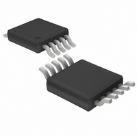
LTC4214-1CMS#PBF Linear Technology, LTC4214-1CMS#PBF Datasheet - Page 16

LTC4214-1CMS#PBF
Manufacturer Part Number
LTC4214-1CMS#PBF
Description
IC CTRLR HOTSWAP NEGVOLT 10MSOP
Manufacturer
Linear Technology
Type
Hot-Swap Controllerr
Datasheet
1.LTC4214-1CMS.pdf
(32 pages)
Specifications of LTC4214-1CMS#PBF
Applications
General Purpose
Internal Switch(s)
No
Voltage - Supply
6 V ~ 16 V
Operating Temperature
0°C ~ 70°C
Mounting Type
Surface Mount
Package / Case
10-TFSOP, 10-MSOP (0.118", 3.00mm Width)
Linear Misc Type
Negative Low Voltage
Family Name
LTC4214-1
Package Type
MSOP
Operating Supply Voltage (min)
-6V
Operating Supply Voltage (max)
-16V
Operating Temperature (min)
0C
Operating Temperature (max)
70C
Operating Temperature Classification
Commercial
Product Depth (mm)
3mm
Product Height (mm)
0.86mm
Product Length (mm)
3mm
Mounting
Surface Mount
Pin Count
10
Lead Free Status / RoHS Status
Lead free / RoHS Compliant
Available stocks
Company
Part Number
Manufacturer
Quantity
Price
APPLICATIO S I FOR ATIO
LTC4214-1/LTC4214-2
GATE
GATE is pulled low to V
conditions: in UVLO, in an undervoltage condition, in an
overvoltage condition, during the initial timing cycle or
when the circuit breaker fault times out. When GATE turns
on, a 50 A current source charges the MOSFET gate and
any associated external capacitance. The gate drive is
limited to no more than V
Gate-drain capacitance (C
abrupt application of power can cause a gate-source
voltage sufficient to turn on the MOSFET. A unique circuit
pulls GATE low with practically no usable voltage at V
and eliminates current spikes at insertion. A large external
gate-source capacitor is thus unnecessary for the purpose
of compensating C
capacitor C
for the analog current limit loop.
GATE has two comparators: the GATE low comparator
looks for < 0.5V threshold prior to initial timing or a GATE
start-up cycle; the GATE high comparator looks for < 2.8V
relative to V
tor, sets PWRGD status during GATE start-up.
SENSE
The SENSE pin is monitored by the circuit breaker (CB)
comparator, the analog current limit (ACL) amplifier and
the fast current limit (FCL) comparator. Each of these three
measures the potential of SENSE relative to V
SENSE exceeds 50mV, the CB comparator activates the
40 A TIMER pull-up. At 70mV, the ACL amplifier servos
the MOSFET current and, at 200mV, the FCL comparator
abruptly pulls GATE low in an attempt to bring the MOSFET
current under control. If any of these conditions persists
long enough for TIMER to charge C
tion 3), the LTC4214 shuts down and pulls GATE low.
If the SENSE pin encounters a voltage greater than 70mV,
the ACL amplifier will servo GATE downwards in an
attempt to control the MOSFET current. Since GATE
16
C
IN
is adequate. C
and, together with the DRAIN low compara-
U
GD
. Instead, a smaller value ( 5nF)
EE
IN
U
C
GD
.
also provides compensation
under any of the following
) feedthrough at the first
W
T
to 3V (see Equa-
U
EE
. When
IN
overdrives the MOSFET in normal operation, the ACL
amplifier needs time to discharge GATE to the threshold
of the MOSFET. For a mild overload the ACL amplifier can
control the MOSFET current, but in the event of a severe
overload the current may overshoot. At SENSE = 200mV
the FCL comparator takes over, quickly discharging the
GATE pin to near V
ACL amplifier takes over. All the while TIMER is running.
The effect of FCL is to add a nonlinear response to the
control loop in favor of reducing MOSFET current.
Owing to inductive effects in the system, FCL typically
overcorrects the current limit loop and GATE under-
shoots. A zero in the loop (resistor R
gate capacitor) helps the ACL amplifier to recover.
SHORT-CIRCUIT OPERATION
Circuit behavior arising from a load side low impedance
short is shown in Figure 5 for the LTC4214. Initially, the
current overshoots the fast current limit level of V
200mV (Trace 2) as the GATE pin works to bring V
control (Trace 3). The overshoot glitches the backplane in
the negative direction and when the current is reduced to
70mV/R
positive direction.
RESPECT TO –12V
GND WITH
Figure 5. Output Short-Circuit Behavior of LTC4214
S
200mV
SENSE
TIMER
0.1ms
0.1ms
0.1ms
0.1ms
, the backplane responds by glitching in the
GATE
10V
10V
2V
OWING TO CURRENT
SUPPLY RING
OVERSHOOT
EE
FAST
CURRENT
LIMIT
potential. FCL then releases and the
ONSET OF OUTPUT
SHORT CIRCUIT
C
TIMER
RAMP
OWING TO MOSFET
CURRENT
ANALOG
LIMIT
SUPPLY RING
TURN-OFF
LATCH OFF
C
in series with the
4214 F05
TRACE 1
TRACE 2
TRACE 3
TRACE 4
GS
SENSE
under
421412f
=


