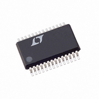
LTC4240CGN Linear Technology, LTC4240CGN Datasheet - Page 26

LTC4240CGN
Manufacturer Part Number
LTC4240CGN
Description
IC CTRLR HOTSWAP CPCI I2C 28SSOP
Manufacturer
Linear Technology
Type
Hot-Swap Controllerr
Datasheet
1.LTC4240CGNPBF.pdf
(28 pages)
Specifications of LTC4240CGN
Applications
CompactPCI™
Internal Switch(s)
No
Voltage - Supply
3.3V, 5V, ±12V
Operating Temperature
0°C ~ 70°C
Mounting Type
Surface Mount
Package / Case
28-SSOP (0.150", 3.95mm Width)
Lead Free Status / RoHS Status
Contains lead / RoHS non-compliant
Available stocks
Company
Part Number
Manufacturer
Quantity
Price
Part Number:
LTC4240CGN
Manufacturer:
LINEAR/凌特
Quantity:
20 000
LTC4240
APPLICATIO S I FOR ATIO
*ADDITIONAL DETAILS OMITTED FOR CLARITY. DRAWING IS NOT TO SCALE!
26
Note (see front page schematic) that the 12V and –12V
show 0.01 F snubber capacitors. This is consistent with
the CPCI specification since we also recommend a 10
snubber resistor. The 12V
high energy large voltage transients. A transient voltage
suppressor with a breakdown voltage between 13.2V and
15V is advisable. The TVS should also be able to dissipate
at least 150W. The SMAJ12CA can be used for both 12V
and V
page schematic.
5V
GND
5V
EEIN
IN
Figure 18. Recommended Layout for Power MOSFET,
Sense Resistor and GATE Components for the 5V Rail.
Similar Layout for 3.3V Rail Not Shown
C
TRACK WIDTH W:
0.03" PER AMPERE
ON 1OZ Cu FOIL
TIMER
CURRENT FLOW
. Place the TVS close to the LTC4240. See front
TO LOAD
W
W
RESISTOR
U
SENSE
LTC4240CGN*
U
IN
GATE
pin is the most sensitive to
CURRENT FLOW
TO SOURCE
D
D
D
D
R4
R5
W
MOSFET
POWER
C1
G
S
S
S
CURRENT FLOW
SIMILAR LAYOUT
FOR 3.3V RAIL
NOT SHOWN
TO LOAD
U
VIA TO
GND PLANE
W
VIA/PATH
TO GND
4240 F18
GND
5V
5V
IN
OUT
PCB Layout Considerations
For proper operation of the LTC4240’s circuit breaker
function, a 4-wire Kelvin connection to the sense resistors
is highly recommended. A recommended PCB layout for
the sense resistor, the power MOSFET, and the GATE drive
components around the LTC4240 is illustrated in
Figure 18. The drawing is not to scale and is only intended
to show the low resistance, external high current path. In
hot swap applications where load currents can reach 10A,
narrow PCB tracks exhibit more resistance than wider
tracks and operate at more elevated temperatures. Since
the sheet resistance of 1 ounce copper is approximately
0.5m /square, track resistances add up quickly in high-
current applications. Thus, to keep PCB track resistance
and temperature rise to a minimum, the suggested trace
width in these applications for 1 ounce copper is 0.03" for
each ampere of DC current.
In order to help dissipate the heat generated by the power
MOSFET, the copper trace connected to the drain should
be made as large as possible.
In the majority of applications, it will be necessary to use
plated-through vias to make circuit connections from
component layers to power and ground layers internal to
the PC board. For 1 ounce copper plating, a general rule is
1A of DC current per via, making sure the via is properly
dimensioned so that solder completely fills any void. For
other plating thicknesses, check with your PCB fabrication
facility.
Power MOSFET and Sense Resistor Selection
Table 7 lists some current MOSFET transistors that are
available. Table 8 lists some current sense resistors that
can be used with the LTC4240’s circuit breakers. Table 9
lists supplier web site addresses for discrete components
mentioned throughout the LTC4240 data sheet. High
current applications should select a MOSFET with very
low on-resistance and good transient thermal character-
istics.
4240f


