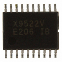
X9522V20I-B Intersil, X9522V20I-B Datasheet - Page 6

X9522V20I-B
Manufacturer Part Number
X9522V20I-B
Description
IC TRIPL DCP LASER CNTRL 20TSSOP
Manufacturer
Intersil
Type
Laser Diode Controller (Fiber Optic)r
Datasheet
1.X9522V20I-A.pdf
(29 pages)
Specifications of X9522V20I-B
Number Of Channels
3
Voltage - Supply
2.7 V ~ 5.5 V
Current - Supply
1.5mA
Operating Temperature
-40°C ~ 85°C
Package / Case
20-TSSOP
Mounting Type
Surface Mount
Lead Free Status / RoHS Status
Contains lead / RoHS non-compliant
DEVICE INTERNAL ADDRESSING
Addressing Protocol Overview
The user addressable internal components of the
X9522 can be split up into two main parts:
—Three Digitally Controlled Potentiometers (DCPs)
—Control and Status (CONSTAT) Register
Depending upon the operation to be performed
on each of these individual parts, a 1, 2 or 3 Byte
protocol is used. All operations however must
begin with the Slave Address Byte being issued
on the SDA pin. The Slave address selects the
part of the X9522 to be addressed, and specifies
if a Read or Write operation is to be performed.
It should be noted that in order to perform a write
operation to a DCP, the Write Enable Latch (WEL)
bit must first be set.
Slave Address Byte
Following a START condition, the master must
output a Slave Address Byte (Refer to Figure 4.).
This byte consists of three parts:
—The Device Type Identifier which consists of the most
significant four bits of the Slave Address (SA7 - SA4).
The Device Type Identifier must always be set to 1010
in order to select the X9522.
Data Output
Data Output
Transmitter
Receiver
Master
Master
from
from
from
from
SCL
SCL
Start
6
Figure 3.
Acknowledge Response From Receiver
1
X9522
—The next three bits (SA3 - SA1) are the Internal Device
—The Least Significant Bit of the Slave Address (SA0)
Address bits. Setting these bits to 111 internally selects
the DCP structures in the X9522. The CONSTAT Reg-
ister may be selected using the Internal Device
Address
RESERVED.
Byte is the R/W bit. This bit defines the operation to be
performed on the device being addressed (as defined
in the bits SA3 - SA1). When the R/W bit is “1”, then a
READ operation is selected. A “0” selects a WRITE
operation (Refer to Figure 4.)
Figure 4.
SA7
1 0 1 0
Internal Address
DEVICE TYPE
(SA3 - SA1)
IDENTIFIER
8
Bit SA0
Others
SA6
010
111
010.All
0
1
SA5
Slave Address Format
Acknowledge
SA4
other
9
SA3
Internally Addressed
CONSTAT Register
bit
INTERNAL
ADDRESS
DEVICE
RESERVED
SA2
Operation
Device
WRITE
READ
DCP
combinations
SA1
September 7, 2010
READ /
WRITE
R/W
SA0
FN8208.2
are


