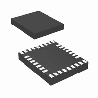
LP3950SL/NOPB National Semiconductor, LP3950SL/NOPB Datasheet - Page 13

LP3950SL/NOPB
Manufacturer Part Number
LP3950SL/NOPB
Description
IC LED DRVR WHITE BCKLGT 32-TSCP
Manufacturer
National Semiconductor
Series
PowerWise®r
Type
Backlight, White LED (I²C Interface)r
Datasheet
1.LP3950SLNOPB.pdf
(31 pages)
Specifications of LP3950SL/NOPB
Topology
PWM, Step-Up (Boost)
Number Of Outputs
6
Internal Driver
Yes
Type - Primary
Flash/Torch, LED Blinker, Light Management Unit (LMU)
Type - Secondary
RGB, White LED
Frequency
2MHz
Voltage - Supply
2.7 V ~ 2.9 V
Voltage - Output
5V
Mounting Type
Surface Mount
Package / Case
32-Laminate TCSP
Operating Temperature
-40°C ~ 85°C
Internal Switch(s)
Yes
Efficiency
90%
Led Driver Application
Mobile Phone Display Lighting, General LED Lighting
No. Of Outputs
6
Output Current
300mA
Output Voltage
5.3V
Input Voltage
3V To 7.2V
Rohs Compliant
Yes
Lead Free Status / RoHS Status
Lead free / RoHS Compliant
Current - Output / Channel
-
Other names
LP3950SL/CSP1
LP3950SLTR
LP3950SLTR
I
V
Symbol
LOAD
OUT
Magnetic Boost DC/DC Converter
The boost DC/DC converter generates a 4.1V–5.3V output voltage to drive LEDs from a single Li-Ion battery (3.0V to 4.5V). The
output voltage is controlled with an eight-bit register in nine steps. The converter is a magnetic switching PWM mode DC/DC
converter with a current limit. The converter has three options for switching frequency, 1.0 MHz, 1.67 MHz and 2.0 MHz (default),
when the timing resistor RT is 82 kΩ.
The LP3950 boost converter uses an unique pulse-skipping elimination method to stabilize the noise spectrum. Even with light
load or no load a minimum length current pulse is fed to the inductor. An internal active load is used to remove the excess charge
from the output capacitor when needed (Note 16). The boost converter should be disabled when there is no load to avoid idle
current consumption.
The topology of the magnetic boost converter is called CPM control, current programmed mode, where the inductor current is
measured and controlled with the feedback. The output voltage control changes the resistor divider in the feedback loop.
Figure 11 shows the boost topology with the protection circuitry. Four different protection schemes are implemented:
1. Over voltage protection, limits the maximum output voltage
2. Over current protection, limits the maximum inductor current
3.
4. Duty cycle limit function, done with digital control
Note 16: When the battery voltage is close to the output voltage, the output voltage may rise slightly over programmed value if the load on output is small and
pulse-skipping elimination is active.
Magnetic Boost DC/DC Converter Electrical Characteristics
Limits in standard typeface are for T
(−40˚C ≤ T
C
VDD2
— Keeps the output below breakdown voltage
— Prevents boost operation if the battery voltage is much higher than desired output
— Voltage over switching NMOS is monitored; too high voltages turn the switch off
Feedback (FB) protection for no connection
= C
Load Current
Output Voltage Accuracy
(FB Pin)
Output Voltage
(FB Pin)
VDDA
A
≤ +85˚C). Unless otherwise noted, specifications apply to Figure 1 with: V
= C
Parameter
VDDIO
= 100 nF, C
FIGURE 11. Boost Converter Functional Block Diagram
J
= +25˚C. Limits in boldface type apply over the operating ambient temperature range
OUT
3.0V ≤ V
V
1.0 mA ≤ I
3.0V ≤ V
V
1.0 mA ≤ I
3.0V
autoload OFF
1.0 mA ≤ I
V
OUT
OUT
IN
= C
>
<
= 5.0V
= 5.0V (target value), autoload OFF
5V + V
IN
V
IN
IN
IN
= 10 µF, C
LOAD
LOAD
LOAD
≤ 4.5V
≤ 4.5V
<
(SCHOTTKY)
5.0V + V
Conditions
≤ 300 mA
≤ 300 mA
≤ 300 mA
VREF
(SCHOTTKY),
13
= 100 nF, L
1
= 4.7 µH and f
Min
−5
0
DD1
= V
V
BOOST
IN
DD2
20129315
–V
= V
(SCHOTTKY)
Typ
5.0
= 2.0 MHz (Note 12).
DDA
= 2.8V, C
Max
300
+5
www.national.com
VDD1
=
Units
mA
%
V
V


