LP3950SL/NOPB National Semiconductor, LP3950SL/NOPB Datasheet - Page 4
LP3950SL/NOPB
Manufacturer Part Number
LP3950SL/NOPB
Description
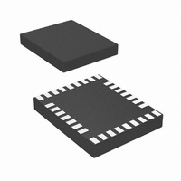
IC LED DRVR WHITE BCKLGT 32-TSCP
Manufacturer
National Semiconductor
Series
PowerWise®r
Type
Backlight, White LED (I²C Interface)r
Datasheet
1.LP3950SLNOPB.pdf
(31 pages)
Specifications of LP3950SL/NOPB
Topology
PWM, Step-Up (Boost)
Number Of Outputs
6
Internal Driver
Yes
Type - Primary
Flash/Torch, LED Blinker, Light Management Unit (LMU)
Type - Secondary
RGB, White LED
Frequency
2MHz
Voltage - Supply
2.7 V ~ 2.9 V
Voltage - Output
5V
Mounting Type
Surface Mount
Package / Case
32-Laminate TCSP
Operating Temperature
-40°C ~ 85°C
Internal Switch(s)
Yes
Efficiency
90%
Led Driver Application
Mobile Phone Display Lighting, General LED Lighting
No. Of Outputs
6
Output Current
300mA
Output Voltage
5.3V
Input Voltage
3V To 7.2V
Rohs Compliant
Yes
Lead Free Status / RoHS Status
Lead free / RoHS Compliant
Current - Output / Channel
-
Other names
LP3950SL/CSP1
LP3950SLTR
LP3950SLTR


www.national.com
I
I
I
V
VDD
VDDIO
VDDA
Symbol
REF
Absolute Maximum Ratings
2)
If Military/Aerospace specified devices are required,
please contact the National Semiconductor Sales Office/
Distributors for availability and specifications.
Electrical Characteristics
Limits in standard typeface are for T
(−40˚C ≤ T
C
Note 1: Absolute Maximum Ratings indicate limits beyond which damage to the component may occur. Operating Ratings are conditions under which operation of
the device is guaranteed. Operating Ratings do not imply guaranteed performance limits. For guaranteed performance limits and associated test conditions, see the
Electrical Characteristics tables.
Note 2: All voltages are with respect to the potential at the GND pins (GND1–3, GND_BOOST, GND_RGB, GNDA).
Note 3: Battery/Charger voltage should be above 6.0V no more than 10% of the operational lifetime.
Note 4: Voltage tolerance of LP3950 above 6.0V relies on fact that V
not available (ON) at all conditions, National Semiconductor does not guarantee any parameters or reliability for this device. Also, V
at the same electric potential.
Note 5: The total load current of the boost converter should be limited to 300 mA.
Note 6: Internal thermal shutdown circuitry protects the device from permanent damage. Thermal shutdown engages at T
140˚C (typ.).
Note 7: For detailed package and soldering specifications and information, please refer to National Semiconductor Application Note 1125: Laminate CSP/FBGA.
Note 8: The Human body model is a 100 pF capacitor discharged through a 1.5 kΩ resistor into each pin. The machine model is a 200 pF capacitor discharged
directly into each pin. MIL-STD-883 3015.7
V (SW, FB, R1–2, G1–2, B1–2)
V
Voltage on ASE, AD1, AD2
Voltage on Logic Pins
I (R1, G1, B1, R2, G2, B2)
I (V
Continuous Power Dissipation
Junction Temperature (T
Storage Temperature Range
VDD2
DD1
(Notes 3, 4)
(Note 5)
(Note 6)
REF
, V
= C
)
DD2
Standby Supply Current
(V
No-Load Supply Current
(V
off)
Full Load Supply Current
(V
on)
(Note 13)
V
Audio Circuitry Supply Current
(Note 14)
Reference Voltage(Note 15)
VDDA
A
DDIO
, V
DD1
DD1
DD1
≤ +85˚C). Unless otherwise noted, specifications apply to Figure 1 with: V
DDIO
= C
+ V
+ V
+ V
Supply Current
, V
VDDIO
DD2
DD2
DD2
DDA
Parameter
+ V
+ V
+ V
J-MAX
= 100 nF, C
DDA
DDA
DDA
)
V
current, boost
current)
current, boost
DD1
J
+0.3V with 6.0V max
+0.3V with 6.0V max
= +25˚C. Limits in boldface type apply over the operating ambient temperature range
OUT
Internally Limited
−65˚C to +150˚C
−0.3V to V
= C
−0.3V to +7.2V
−0.3V to +6.0V
(Notes 2, 11)
IN
(Notes 1,
= 10 µF, C
−0.3V to
150 mA
NSTBY = L (register)
SCK, SS, SI, NRST = H
NSTBY = H (reg.)
EN_BOOST = L (reg.)
SCK, SS, SI, NRST = H
NSTBY = H (reg.)
EN_BOOST = H (reg.)
SCK, SS, SI, NRST = H
All Outputs Active
1.0 MHz SCK Frequency
C
INPUT_SEL = [10] (register)
I
Purpose
REF
125˚C
10 µA
L
DD_IO
= 50 pF at SO Pin
DD1
≤ 1.0 nA Only for Test
, V
DD2
VREF
Condition
4
and V
= 100 nF, L
Operating Ratings
Thermal Properties
DDA
Maximum Lead Temperature
(Reflow soldering, 3 times) (Note 7)
ESD Rating (Note 8)
V (SW, FB, R1–2, G1–2, B1–2)
V
V
Voltage on ASE, AD1, AD2
Recommended Load Current
Junction Temperature (T
Ambient Temperature (T
Junction-to-Ambient Thermal Resistance
DD1
DDIO
Human Body Model:
Machine Model:
(Note 9)
(2.8V) are available (ON) at all conditions. If V
(θ
, V
JA
), SLD32A Package (Note 10)
DD2
1
= 4.7 µH and f
, V
DDA
DD1
(Note 4)
Min
= V
A
J
BOOST
) Range
) Range
DD2
J
= 160˚C (typ.) and disengages at T
1.230
(Notes 1, 2)
= V
Typ
300
850
550
20
= 2.0 MHz (Note 12).
1
DDA
DD1
0.1V to V
, V
= 2.8V, C
1.65V to V
DD1
−40˚C to +125˚C
DD2
0 mA to 300 mA
−40˚C to +85˚C
, V
Max
400
5
and V
DD2
2.7V to 2.9V
0V to 6.0V
DD1
and V
VDD1
DDA
72˚C/W
DD1,2
260˚C
- 0.1V
200V
must be
DDA
2 kV
Units
=
µA
µA
µA
µA
µA
V
V
are
J
=
Related parts for LP3950SL/NOPB
Image
Part Number
Description
Manufacturer
Datasheet
Request
R

Part Number:
Description:
Color LED Driver with Audio Synchronizer
Manufacturer:
NSC [National Semiconductor]
Datasheet:

Part Number:
Description:
National Semiconductor [8-Bit D/A Converter]
Manufacturer:
National Semiconductor
Datasheet:
Part Number:
Description:
National Semiconductor [Media Coprocessor]
Manufacturer:
National Semiconductor
Datasheet:
Part Number:
Description:
Digitally Controlled Tone and Volume Circuit with Stereo Audio Power Amplifier, Microphone Preamp Stage and National 3D Sound
Manufacturer:
National Semiconductor
Datasheet:
Part Number:
Description:
Digitally Controlled Tone and Volume Circuit with Stereo Audio Power Amplifier, Microphone Preamp Stage and National 3D Sound
Manufacturer:
National Semiconductor
Datasheet:
Part Number:
Description:
AC97 Rev 2 Codec with Sample Rate Conversion and National 3D Sound
Manufacturer:
National Semiconductor
Part Number:
Description:
Manufacturer:
National Semiconductor
Datasheet:
Part Number:
Description:
Manufacturer:
National Semiconductor
Datasheet:
Part Number:
Description:
General Purpose, Low Voltage, Low Power, Rail-to-Rail Output Operational Amplifiers
Manufacturer:
National Semiconductor
Datasheet:
Part Number:
Description:
8-bit 20 MSPS flash A/D converter.
Manufacturer:
National Semiconductor
Datasheet:
Part Number:
Description:
Low Noise Quad Operational Amplifier
Manufacturer:
National Semiconductor
Datasheet:
Part Number:
Description:
Quad Differential Line Receivers
Manufacturer:
National Semiconductor
Datasheet:
Part Number:
Description:
Quad High Speed Trapezoidal? Bus Transceiver
Manufacturer:
National Semiconductor
Datasheet:
Part Number:
Description:
Dual Line Receiver
Manufacturer:
National Semiconductor
Datasheet: