LP3950SL/NOPB National Semiconductor, LP3950SL/NOPB Datasheet - Page 14
LP3950SL/NOPB
Manufacturer Part Number
LP3950SL/NOPB
Description
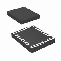
IC LED DRVR WHITE BCKLGT 32-TSCP
Manufacturer
National Semiconductor
Series
PowerWise®r
Type
Backlight, White LED (I²C Interface)r
Datasheet
1.LP3950SLNOPB.pdf
(31 pages)
Specifications of LP3950SL/NOPB
Topology
PWM, Step-Up (Boost)
Number Of Outputs
6
Internal Driver
Yes
Type - Primary
Flash/Torch, LED Blinker, Light Management Unit (LMU)
Type - Secondary
RGB, White LED
Frequency
2MHz
Voltage - Supply
2.7 V ~ 2.9 V
Voltage - Output
5V
Mounting Type
Surface Mount
Package / Case
32-Laminate TCSP
Operating Temperature
-40°C ~ 85°C
Internal Switch(s)
Yes
Efficiency
90%
Led Driver Application
Mobile Phone Display Lighting, General LED Lighting
No. Of Outputs
6
Output Current
300mA
Output Voltage
5.3V
Input Voltage
3V To 7.2V
Rohs Compliant
Yes
Lead Free Status / RoHS Status
Lead free / RoHS Compliant
Current - Output / Channel
-
Other names
LP3950SL/CSP1
LP3950SLTR
LP3950SLTR


www.national.com
RDS
f
t
t
I
Symbol
PWF
PULSE
STARTUP
CL_OUT
Magnetic Boost DC/DC Converter Electrical Characteristics
Limits in standard typeface are for T
(−40˚C ≤ T
C
Boost Standby Mode
User can set the boost converter to STANDBY mode by writing the register bit EN_BOOST low when there is no load to avoid
idle current consumption. When EN_BOOST is written high, the converter starts in PFM (Pulse Frequency Modulation) mode for
10 ms and then goes to PWM (Pulse Width Modulation ) mode. All RGB outputs are off during the 10 ms delay.
Boost Output Voltage Control
User can control the boost output voltage by eight-bit boost output voltage register according to the following table.
Boost Frequency Control
The register ‘boost frequency’ has address 0C’h. The default value after reset is 07’h. ‘x’ means don’t care.
VDD2
ON
= C
Switch ON Resistance
PWM Mode Switching
Frequency
Frequency Accuracy
Switch Pulse Minimum
Width
Startup Time
SW Pin Current Limit
0000 0000
0000 0001
0000 0011
0000 0111
0000 1111
FREQ_SEL[2:0]
VDDA
Register 0D’h
A
Binary
BOOST[7:0]
≤ +85˚C). Unless otherwise noted, specifications apply to Figure 1 with: V
= C
1xx
01x
Parameter
VDDIO
Hex
0F
00
01
03
07
= 100 nF, C
BOOST Output
Frequency
2.00 MHz
1.67 MHz
J
(typical)
Voltage
= +25˚C. Limits in boldface type apply over the operating ambient temperature range
OUT
V
RT = 82 kΩ
freq_sel[2:0] = 1XX
2.7 ≤ VDD
RT = 82 kΩ
No Load
4.10
4.25
4.40
4.55
4.70
DD1,2
= C
= 2.8V, I
IN
= 10 µF, C
1,2
≤ 2.9
Conditions
SW
= 0.5A
VREF
14
= 100 nF, L
0001 1111
0011 1111
0111 1111
1111 1111
1
FREQ_SEL[2:0]
Register 0D’h
Binary
= 4.7 µH and f
BOOST[7:0]
001
Min
700
500
−6
−9
DD1
= V
Hex
1F
3F
7F
FF
BOOST
DD2
= V
Typ
800
0.4
2.0
±
25
15
= 2.0 MHz (Note 12).
BOOST Output
(Continued)
3
5.00 Default
Frequency
DDA
1.00 MHz
(typical)
Voltage
4.85
5.15
5.30
= 2.8V, C
1000
Max
900
0.7
+6
+9
VDD1
=
Units
MHz
mA
ms
ns
%
Ω
Related parts for LP3950SL/NOPB
Image
Part Number
Description
Manufacturer
Datasheet
Request
R

Part Number:
Description:
Color LED Driver with Audio Synchronizer
Manufacturer:
NSC [National Semiconductor]
Datasheet:

Part Number:
Description:
National Semiconductor [8-Bit D/A Converter]
Manufacturer:
National Semiconductor
Datasheet:
Part Number:
Description:
National Semiconductor [Media Coprocessor]
Manufacturer:
National Semiconductor
Datasheet:
Part Number:
Description:
Digitally Controlled Tone and Volume Circuit with Stereo Audio Power Amplifier, Microphone Preamp Stage and National 3D Sound
Manufacturer:
National Semiconductor
Datasheet:
Part Number:
Description:
Digitally Controlled Tone and Volume Circuit with Stereo Audio Power Amplifier, Microphone Preamp Stage and National 3D Sound
Manufacturer:
National Semiconductor
Datasheet:
Part Number:
Description:
AC97 Rev 2 Codec with Sample Rate Conversion and National 3D Sound
Manufacturer:
National Semiconductor
Part Number:
Description:
Manufacturer:
National Semiconductor
Datasheet:
Part Number:
Description:
Manufacturer:
National Semiconductor
Datasheet:
Part Number:
Description:
General Purpose, Low Voltage, Low Power, Rail-to-Rail Output Operational Amplifiers
Manufacturer:
National Semiconductor
Datasheet:
Part Number:
Description:
8-bit 20 MSPS flash A/D converter.
Manufacturer:
National Semiconductor
Datasheet:
Part Number:
Description:
Low Noise Quad Operational Amplifier
Manufacturer:
National Semiconductor
Datasheet:
Part Number:
Description:
Quad Differential Line Receivers
Manufacturer:
National Semiconductor
Datasheet:
Part Number:
Description:
Quad High Speed Trapezoidal? Bus Transceiver
Manufacturer:
National Semiconductor
Datasheet:
Part Number:
Description:
Dual Line Receiver
Manufacturer:
National Semiconductor
Datasheet: