LM2759SD/NOPB National Semiconductor, LM2759SD/NOPB Datasheet - Page 3
LM2759SD/NOPB
Manufacturer Part Number
LM2759SD/NOPB
Description
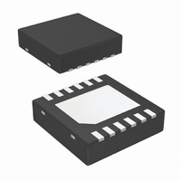
IC LED DRIVER PHOTO FLASH 12-LLP
Manufacturer
National Semiconductor
Series
PowerWise®r
Type
Photo Flash LED (I²C Interface)r
Datasheet
1.LM2759SDNOPB.pdf
(14 pages)
Specifications of LM2759SD/NOPB
Constant Current
Yes
Topology
Switched Capacitor (Charge Pump)
Number Of Outputs
1
Internal Driver
Yes
Type - Primary
Flash/Torch
Frequency
700kHz ~ 1.3MHz
Voltage - Supply
*
Voltage - Output
2 V ~ 4 V
Mounting Type
Surface Mount
Package / Case
12-LLP
Operating Temperature
-30°C ~ 85°C
Current - Output / Channel
1A
Internal Switch(s)
Yes
Efficiency
90%
Led Driver Application
Camera Flash In Mobile Phones, Flash For Digital Cameras
No. Of Outputs
1
Output Current
1A
Output Voltage
5.1V
Input Voltage
2.7V To 5.5V
Rohs Compliant
Yes
Lead Free Status / RoHS Status
Lead free / RoHS Compliant
Other names
LM2759SDTR
Available stocks
Company
Part Number
Manufacturer
Quantity
Price
Company:

Part Number:
LM2759SD/NOPB
Manufacturer:
National Semiconductor
Quantity:
1 790


I
I
V
V
R
F
V
V
I
I
LED
FLASH
Q
SD
Symbol
SW
GDX
OUT
IH
IL
OUT
Absolute Maximum Ratings
3)
If Military/Aerospace specified devices are required,
please contact the National Semiconductor Sales Office/
Distributors for availability and specifications.
ESD Caution Notice
National Semiconductor recommends that all integrated circuits be handled with appropriate ESD precautions. Failure to observe
proper ESD handling techniques can result in damage to the device.
Electrical Characteristics
Limits in standard typeface are for T
C
V
V
Strobe, TX, SDA, SCL, I
Voltage to GND
Continuous Power Dissipation
(Note
Junction Temperature (T
Storage Temperature Range
Maximum Lead Temp. (Soldering)
ESD
Human Body Model
TX
≤
IN
= 0V, V
T
pin: Voltage to GND
J
Rating(Note
4)
≤
+125 °C). Unless otherwise noted, specifications apply to the LM2759 Typical Application Circuit (pg.1) with V
LED Current Sink
Accuracy
Max Flash Output Current Flash Mode
Gain Transition Voltage
Threshold on I
Output Voltage
x1 Mode Output
Impedance
1.5x Mode Output
Impedance
x2 Mode Output
Impedance
Switching Frequency
Input Logic High
Input Logic Low
Quiescent Current
Shutdown Current
STROBE
Parameter
6)
= 0V, C
SINK
SINK
J-MAX
IN
= C
pins:
)
1
= C
J
= 25°C. Limits in boldface type apply over the full operating junction temperature range (-30°
2
Flash Mode
ADDR xB0 = 0x02
ADDR xB0 = 0x0F
I
(V
1x Mode, I
1.5x Mode, I
2x Mode, I
I
I
2.7V
Pins: TX, Strobe
Pins: TX, Strobe
I
I
I
Device Disabled
2.7V
LED
OUT
OUT
OUT
OUT
OUT
-0.3V to (V
= 2.2 µF, C
ISINK
= 500mA
= 200mA, V
= 500mA, V
= 0 mA, 1x Mode
= 0 mA, 1.5x Mode
= 0 mA, 2x Mode
Internally Limited
≤
≤
-65°C to 150°C
(Note
falling)
V
V
-0.3V to 6.0V
IN
IN
w/ 6.0V max
(Note
OUT
OUT
≤
≤
IN
OUT
OUT
3,
5.5V
5.5V
(Note
+ 0.3V)
= 0 mA (V
= 0 mA
2,
150°C
2.5KV
Note
= 0 mA
IN
IN
= 4.7 µF.
Conditions
Note
= 3.3V
= 3.3V
5)
9)
IN
3
(Note
>V
OUT
Operating Ratings
Thermal Information
Input Voltage Range
LED Voltage Range
Junction Temperature Range (T
Ambient Temperature Range (T
(Note
Junction-to-Ambient Thermal Resistance
(θ
10)
)(Note
JA
), Leadless Leadframe Package
7)
12)
−10%
1.26
Min
198
0.7
0.33
2.25
Typ
220
350
4.7
4.7
5.1
1.9
0.6
3.4
5.9
5.8
1
1
A
(Note
J
)
)
(Note
2,
Note
+10%
-30°C to +125°C
Max
242
8)
4.9
4.9
5.4
1.3
0.7
0.9
4.0
7.0
9.7
-30°C to +85°C
3)
2.7V to 5.5V
2.0V to 4.0V
www.national.com
36.7°C/W
IN
= 3.6V,
Units
MHz
mA
mV
mA
µA
A
V
Ω
V
V
Related parts for LM2759SD/NOPB
Image
Part Number
Description
Manufacturer
Datasheet
Request
R

Part Number:
Description:
National Semiconductor [8-Bit D/A Converter]
Manufacturer:
National Semiconductor
Datasheet:
Part Number:
Description:
National Semiconductor [Media Coprocessor]
Manufacturer:
National Semiconductor
Datasheet:
Part Number:
Description:
Digitally Controlled Tone and Volume Circuit with Stereo Audio Power Amplifier, Microphone Preamp Stage and National 3D Sound
Manufacturer:
National Semiconductor
Datasheet:
Part Number:
Description:
Digitally Controlled Tone and Volume Circuit with Stereo Audio Power Amplifier, Microphone Preamp Stage and National 3D Sound
Manufacturer:
National Semiconductor
Datasheet:
Part Number:
Description:
AC97 Rev 2 Codec with Sample Rate Conversion and National 3D Sound
Manufacturer:
National Semiconductor
Part Number:
Description:
Manufacturer:
National Semiconductor
Datasheet:
Part Number:
Description:
Manufacturer:
National Semiconductor
Datasheet:
Part Number:
Description:
General Purpose, Low Voltage, Low Power, Rail-to-Rail Output Operational Amplifiers
Manufacturer:
National Semiconductor
Datasheet:
Part Number:
Description:
8-bit 20 MSPS flash A/D converter.
Manufacturer:
National Semiconductor
Datasheet:
Part Number:
Description:
Low Noise Quad Operational Amplifier
Manufacturer:
National Semiconductor
Datasheet:
Part Number:
Description:
Quad Differential Line Receivers
Manufacturer:
National Semiconductor
Datasheet:
Part Number:
Description:
Quad High Speed Trapezoidal? Bus Transceiver
Manufacturer:
National Semiconductor
Datasheet:
Part Number:
Description:
Dual Line Receiver
Manufacturer:
National Semiconductor
Datasheet:
Part Number:
Description:
TTL to 10k ECL Level Translator with Latch
Manufacturer:
National Semiconductor
Datasheet: