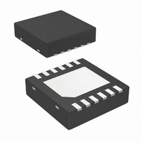
LM2759SD/NOPB National Semiconductor, LM2759SD/NOPB Datasheet - Page 4

LM2759SD/NOPB
Manufacturer Part Number
LM2759SD/NOPB
Description
IC LED DRIVER PHOTO FLASH 12-LLP
Manufacturer
National Semiconductor
Series
PowerWise®r
Type
Photo Flash LED (I²C Interface)r
Datasheet
1.LM2759SDNOPB.pdf
(14 pages)
Specifications of LM2759SD/NOPB
Constant Current
Yes
Topology
Switched Capacitor (Charge Pump)
Number Of Outputs
1
Internal Driver
Yes
Type - Primary
Flash/Torch
Frequency
700kHz ~ 1.3MHz
Voltage - Supply
*
Voltage - Output
2 V ~ 4 V
Mounting Type
Surface Mount
Package / Case
12-LLP
Operating Temperature
-30°C ~ 85°C
Current - Output / Channel
1A
Internal Switch(s)
Yes
Efficiency
90%
Led Driver Application
Camera Flash In Mobile Phones, Flash For Digital Cameras
No. Of Outputs
1
Output Current
1A
Output Voltage
5.1V
Input Voltage
2.7V To 5.5V
Rohs Compliant
Yes
Lead Free Status / RoHS Status
Lead free / RoHS Compliant
Other names
LM2759SDTR
Available stocks
Company
Part Number
Manufacturer
Quantity
Price
Company:
Part Number:
LM2759SD/NOPB
Manufacturer:
National Semiconductor
Quantity:
1 790
www.national.com
I
V
V
V
I
t
t
t
t
t
2
2
1
2
3
4
5
Symbol
C Compatible Interface Voltage Specifications (SCL, SDA).
IL
IH
OL
C Compatible Interface Timing Voltage Specifications (SCL, SDA)
Limits in standard typeface are for T
C
V
Note 2: Absolute Maximum Ratings indicate limits beyond which damage to the component may occur. Operating Ratings are conditions under which operation
of the device is guaranteed. Operating Ratings do not imply guaranteed performance limits. For guaranteed performance limits and associated test conditions,
see the Electrical Characteristics tables.
Note 3: All voltages are with respect to the potential to the GND pin.
Note 4: Internal thermal shutdown circuitry protects the device from permanent damage. Thermal shutdown engages at T
120°C (typ.).
Note 5: For detailed soldering specifications and information, please refer to National Semiconductor Application Note AN-1187.
Note 6: The Human body model is a 100 pF capacitor discharged through a 1.5 kΩ resistor into each pin. (MIL-STD-883 3015.7)
Note 7: In applications where high power dissipation and/or poor package thermal resistance is present, the maximum ambient temperature may have to be
derated. Maximum ambient temperature (T
dissipation of the device in the application (P
following equation: T
Note 8: Junction-to-ambient thermal resistance (θ
JEDEC standard JESD51-7. The test board is a 4–layer FR-4 board measuring 102 mm x 76 mm x 1.6 mm with a 2x1 array of thermal vias. The ground plane
on the board is 50 mm x 50 mm. Thickness of copper layers are 53µm/35µm/35µm/53µm (1.5oz/1oz/1oz/1.5oz). Ambient temperature in simulation is 22°C, still
air. Power dissipation is 1W.
The value of θ
environmental conditions. In applications where high maximum power dissipation exists (high V
issues. For more information on these topics, please refer to Application Note 1187: Leadless Leadframe Package (LLP) and the Power Efficiency and Power
Dissipation section of this datasheet.
Note 9: Min and Max limits are guaranteed by design, test, or statistical analysis. Typical (Typ) numbers are not guaranteed, but do represent the most likely
norm. Unless otherwise specified, conditions for Typ specifications are: V
Note 10: C
Note 11: SCL and SDA should be glitch-free in order for proper brightness control to be realized.
Note 12: For input voltage below the regulation target during the gain of 1x, the output voltage will typically be equal to the input voltage.
TX
≤
= 0V, V
T
J
≤
IN
+125 °C). Unless otherwise noted, specifications apply to the LM2759 Typical Application Circuit (pg.1) with V
Input Logic Low “0”
Input Logic High “1'
Output Logic Low “0”
SCL (Clock Period)
Data in Setup Time to SCL
High
Data Out Stable After SCL
Low
SDA Low Setup Time to
SCL Low (Start)
SDA High Hold Time After
SCL High (Stop)
, C
STROBE
JA
OUT
of this product in the LLP package could fall in a range as wide as 30ºC/W to 150ºC/W (if not wider), depending on PWB material, layout, and
, C
A-MAX
Parameter
1
, C
= 0V, C
2
= T
: Low-ESR Surface-Mount Ceramic Capacitors (MLCCs) used in setting electrical characteristics.
J-MAX-OP
IN
= C
- (θ
1
JA
= C
A-MAX
J
× P
D-MAX
= 25°C. Limits in boldface type apply over the full operating junction temperature range (-30°
2.7V
2.7V
I
2
LOAD
D-MAX
) is dependent on the maximum operation junction temperature (T
= 2.2 µF, C
), and the junction-to ambient thermal resistance of the part/package in the application (θ
JA
) is taken from a thermal modeling result, performed under the conditions and guidelines set forth in the
).
≤
≤
= 3 mA
V
V
IN
IN
≤
≤
OUT
5.5V
5.5V
= 4.7 µF.
Conditions
IN
= 3.6V and T
4
(Note
(Note
10)
A
11)
= 25°C.
IN
, high I
OUT
1.25
), special care must be paid to thermal dissipation
Min
100
100
100
2.5
0
J-MAX-OP
J
=150°C (typ.) and disengages at T
= 125ºC), the maximum power
Typ
Max
0.72
300
JA
), as given by the
IN
= 3.6V,
Units
mV
µs
ns
ns
ns
ns
V
V
J
=


