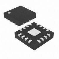
MAX6965ATE+ Maxim Integrated Products, MAX6965ATE+ Datasheet - Page 4

MAX6965ATE+
Manufacturer Part Number
MAX6965ATE+
Description
IC LED DRIVER LINEAR 16-TQFN
Manufacturer
Maxim Integrated Products
Type
Linear (I²C Interface)r
Datasheet
1.MAX6965AEE.pdf
(22 pages)
Specifications of MAX6965ATE+
Topology
Open Drain, PWM
Number Of Outputs
9
Internal Driver
Yes
Type - Primary
Backlight, LED Blinker
Type - Secondary
RGB, White LED
Frequency
400kHz
Voltage - Supply
2 V ~ 3.6 V
Voltage - Output
7V
Mounting Type
Surface Mount
Package / Case
16-TQFN Exposed Pad
Operating Temperature
-40°C ~ 125°C
Current - Output / Channel
50mA
Internal Switch(s)
Yes
Number Of Segments
6
Operating Supply Voltage
2 V to 3.6 V
Maximum Supply Current
110 uA
Maximum Power Dissipation
1176 mW
Maximum Operating Temperature
+ 125 C
Mounting Style
SMD/SMT
Minimum Operating Temperature
- 40 C
Lead Free Status / RoHS Status
Lead free / RoHS Compliant
Efficiency
-
Lead Free Status / Rohs Status
Details
9-Output LED Driver with Intensity Control
and Hot-Insertion Protection
4
TIMING CHARACTERISTICS (continued)
(Typical Operating Circuit, V+ = 2V to 3.6V, T
(Note 1)
Note 1: All parameters tested at T
Note 2: A master device must provide a hold time of at least 300ns for the SDA signal (referred to V
Note 3: Guaranteed by design.
Note 4: C
Note 5: I
Note 6: Input filters on the SDA and SCL inputs suppress noise spikes less than 50ns.
(T
__________________________________________Typical Operating Characteristics
RST Pulse Width
Output Data Valid
A
_______________________________________________________________________________________
0.6
0.5
0.4
0.3
0.2
0.1
= +25°C, unless otherwise noted.)
10
9
8
7
6
5
4
3
2
1
0
0
-40
PORT OUTPUT LOW VOLTAGE WITH 50mA
-40
STANDBY CURRENT vs. TEMPERATURE
the undefined region of SCL’s falling edge.
V+ = 2V
PWM DISABLED
LOAD CURRENT vs. TEMPERATURE
SINK
-25
-25
b
V+ = 2V
= total capacitance of one bus line in pF. t
-10 5 20 35 50
-10 5 20 35 50
V+ = 3.6V
PWM ENABLED
V+ = 2.7V
PWM ENABLED
≤ 6mA. C
TEMPERATURE (°C)
TEMPERATURE (°C)
PARAMETER
V+ = 2.7V
PWM DISABLED
b
V+ = 2.7V
V+ = 3.6V
= total capacitance of one bus line in pF. t
V+ = 2V
PWM ENABLED
65 80
65 80
V+ = 3.6V
PWM
DISABLED
95
95
A
110
110
= +25°C. Specifications over temperature are guaranteed by design.
125
125
A
= T
0.6
0.5
0.4
0.3
0.2
0.1
70
60
50
40
30
20
10
0
0
PORT OUTPUT LOW VOLTAGE WITH 20mA
-40
-40
MIN
SUPPLY CURRENT vs. TEMPERATURE
ALL OUTPUTS LOADED
LOAD CURRENT vs. TEMPERATURE
-25
-25
(PWM DISABLED; f
R
to T
SYMBOL
and t
-10
-10 5 20 35 50
t
t
MAX
DV
W
V+ = 3.6V
5
TEMPERATURE (°C)
F
TEMPERATURE (°C)
, unless otherwise noted. Typical values are at V+ = 3.3V, T
20
measured between 0.3 x V
V+ = 2V
V+ = 2.7V
35
Figure 10
R
50
V+ = 2.7V
and t
SCL
V+ = 2V
65
65 80
= 400kHz)
V+ = 3.6V
80
F
CONDITIONS
measured between 0.3 x V
95
95
110
110
125
125
DD
1.050
1.025
1.000
0.975
0.950
0.925
0.900
70
65
60
55
50
45
40
35
30
25
20
15
10
and 0.7 x V
5
0
-40
-40
SUPPLY CURRENT vs. TEMPERATURE
NORMALIZED TO V+ = 3.3V, T
-25
-25
(PWM ENABLED; f
IL
-10 5 20 35 50
MIN
-10
of the SCL signal) to bridge
PWM CLOCK FREQUENCY
1
DD
V+ = 3.6V
V+ = 2.7V
DD
vs. TEMPERATURE
5
V+ = 3.6V
TEMPERATURE (°C)
and 0.7 x V
TEMPERATURE (°C)
.
20
TYP
35
V+ = 2.7V
50
SCL
V+ = 2V
65 80
V+ = 2V
65
A
MAX
= 400kHz)
DD
= +25°C
5
80
.
A
95
95
= +25°C.)
110
UNITS
110
µs
µs
125
125


