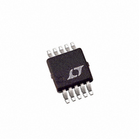
LT3003EMSE#PBF Linear Technology, LT3003EMSE#PBF Datasheet - Page 9

LT3003EMSE#PBF
Manufacturer Part Number
LT3003EMSE#PBF
Description
IC LED DRIVER BALLASTER 10-MSOP
Manufacturer
Linear Technology
Type
LED Ballasterr
Datasheet
1.LT3003EMSEPBF.pdf
(16 pages)
Specifications of LT3003EMSE#PBF
Topology
PWM, Step-Down (Buck), Step-Up (Boost)
Number Of Outputs
3
Internal Driver
Yes
Type - Primary
Automotive, Backlight
Voltage - Supply
3 V ~ 40 V
Mounting Type
Surface Mount
Package / Case
10-MSOP Exposed Pad, 10-HMSOP, 10-eMSOP
Operating Temperature
-40°C ~ 125°C
Current - Output / Channel
350mA
Internal Switch(s)
Yes
Lead Free Status / RoHS Status
Lead free / RoHS Compliant
Voltage - Output
-
Frequency
-
Efficiency
-
Available stocks
Company
Part Number
Manufacturer
Quantity
Price
APPLICATIONS INFORMATION
In addition, LT3003 has an internal 150°C overtemperature
protection circuitry that resets the chip to zero LED current
mode. This prevents the chip from continuous operation
at high temperature.
Thermal Calculations
To maximize output power capability in an application
without exceeding the LT3003 125°C maximum operational
junction temperature, it is useful to be able to calculate
power dissipation within the IC. The power dissipation
within the LT3003 comes from four main sources: switch
DC loss, switch loss due to LED V
quiescent current.
1. Switch DC Loss:
2. Switch Loss due to V
3. Input Quiescent Loss:
4. Total Power Dissipation:
5. LT3003 Junction Temperature:
P
(See (V
Characteristics graph.)
P
P
P
T
θ
I
Q
J
JA
SW(DC)
SW(ΔVLED)
Q
TOT
(LT3003) = T
=
= (V
(P
3
= P
TOT
•
IN
40
LED1,2,3
I
= I
SW(DC)
) = P
LED
– V
LED
= Total V
EE
+
TOT
• V
) • (I
3
A
+ P
– V
mA
+ θ
• 35°C/W
LED
SW(ΔVLED)
Q
EE
LED
JA
LED
– 1mA) + 1mA • V
• 3
) vs I
(P
mismatch • I
TOT
Mismatch:
LED
);
+ P
LED
Typical Performance
Q
mismatch and input
LED
IN
Example
V
Total V
V
Typical Performance Characteristics graph).
1. P
2. P
3. P
4. P
The LT3003 uses a thermally enhanced 10-lead MSE
package. With proper soldering of the Exposed Pad to
the underside of the package, combined with a full copper
plane underneath the device, the thermal resistance (θ
is about 35°C/W. For an ambient temperature of T
the junction temperature of the LT3003, for the example
application described above, can be calculated as:
5. T
Minimizing LT3003 Internal Power Dissipation
The LT3003 requires at least 3V headroom between V
and V
age and low V
in a Buck Mode), it is benefi cial to lower the level of V
pin voltage (LT3003 upper rail) with an external zener to
reduce power dissipation in the chip. Therefore, it is recom-
mended to limit (V
best performance, (V
IN
LED
•
• e.g., LED string 1 voltage drop = 6V;
• Total V
J
= 3V; V
SW(DC)
SW(LED)
Q
TOT
I
Q
= 1.1V at I
EE
= (3 – 0) • (29.25 – 1)mA + 3 • 1mA = 88mW
= T
= 81°C
LED
=
. Hence, for systems with high system input volt-
= 1.1W + 350mW + 88mW ≈1.6W
A
LED string 2 voltage drop = 5.7V;
LED string 3 voltage drop = 5.3V
3 350
LED
mismatch = 1V:
+ θ
EE
= 3 • 350mA • (1.1V) = 1.16W
•
= 1000mV • 350mA = 350mW
40
= 0V; I
JA
mismatch = (6V – 5.7V) + (6V – 5.3V) = 1V
EE
LED
mA
• P
(such as running multiple series LEDs
IN
TOT
LED
= 350mA (see (V
+
IN
– V
3
= 25°C + 35°C/W • 1.6W
– V
mA
= 350mA/string;
EE
) to less than 10V. To achieve
EE
=
) should equal 3V.
29 25
.
mA
LED
– V
LT3003
EE
) vs I
A
= 25°C,
3003fa
9
LED
JA
IN
IN
)


