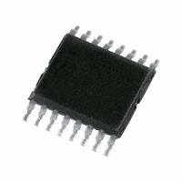
PCA9922PW,112 NXP Semiconductors, PCA9922PW,112 Datasheet - Page 9

PCA9922PW,112
Manufacturer Part Number
PCA9922PW,112
Description
IC LED DRIVER 8-CH 16-TSSOP
Manufacturer
NXP Semiconductors
Type
Linear (Serial Interface)r
Datasheet
1.PCA9922PW112.pdf
(27 pages)
Specifications of PCA9922PW,112
Constant Current
Yes
Number Of Outputs
8
Internal Driver
Yes
Type - Primary
General Purpose
Type - Secondary
Color
Frequency
25MHz
Voltage - Supply
3.3 V ~ 5.5 V
Voltage - Output
5.5V
Mounting Type
Surface Mount
Package / Case
16-TSSOP
Operating Temperature
-40°C ~ 85°C
Current - Output / Channel
60mA
Internal Switch(s)
Yes
Lead Free Status / RoHS Status
Lead free / RoHS Compliant
Efficiency
-
Topology
-
Lead Free Status / Rohs Status
Details
Other names
935285711112
NXP Semiconductors
PCA9922
Product data sheet
7.2.4 Setting the outputs to test
7.2.5 Capturing the fault/output error data
Before the Capture Fault sequence may be performed, the outputs must be set up. A logic
HIGH must be sent to the output control register for all eight bits. This is done after the
Enter Error Detect sequence is performed as a normal data load sequence as seen in
Figure
in the output control register (and the LED[7:0] pins). The output control register will have
to be restored to its proper values by the user after the error detect sequence has been
completed.
The Capture Fault/Error Data sequence can only follow the Enter Error Detect sequence.
If the Error Detect sequence has not occurred, this sequence will be treated as a normal
operational sequence. Once the Capture Fault sequence has occurred, an Exit Error
Detect sequence should be performed. There can be no more Capture Sequences until
another Enter Error Detect sequence has occurred.
The Capture Fault Sequence consists of holding OE LOW for no less than 3 clocks (CLK)
and for a minimum of 2 μs, whichever is longer. During this period of time, the shift register
is being loaded with the fault status. As such, data presented to the device via SDI will not
be captured. Bit 7 of the fault data will be present on SDO by the first falling edge CLK
after the user de-asserts OE for this cycle. An error condition is output as a 1 (HIGH bit),
and a 0 (LOW bit) designates a normal status. Timing for this sequence is shown in
Figure
Fig 7.
5. Please note that this process is completely destructive to the data that is stored
7.
Timing for ‘Capture Fault Mode’ command
All information provided in this document is subject to legal disclaimers.
8-channel constant current LED driver with output error detection
OE = 1'b0 for minimum of 3 clocks
or 2 μs, whichever is longer
SDO
CLK
Rev. 2 — 6 April 2011
OE
LE
previous serial data
fault data MSB
with fault data
resume shift
002aad205
PCA9922
© NXP B.V. 2011. All rights reserved.
9 of 27


