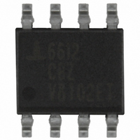
ISL6612CBZ Intersil, ISL6612CBZ Datasheet - Page 6

ISL6612CBZ
Manufacturer Part Number
ISL6612CBZ
Description
IC DRVR MOSF SYNC BUCK OTP 8SOIC
Manufacturer
Intersil
Datasheet
1.ISL6612CBZ.pdf
(12 pages)
Specifications of ISL6612CBZ
Configuration
High and Low Side, Synchronous
Input Type
PWM
Delay Time
10.0ns
Current - Peak
1.25A
Number Of Configurations
1
Number Of Outputs
2
High Side Voltage - Max (bootstrap)
36V
Voltage - Supply
10.8 V ~ 13.2 V
Operating Temperature
0°C ~ 85°C
Mounting Type
Surface Mount
Package / Case
8-SOIC (3.9mm Width)
Lead Free Status / RoHS Status
Lead free / RoHS Compliant
Available stocks
Company
Part Number
Manufacturer
Quantity
Price
Part Number:
ISL6612CBZ
Manufacturer:
INTERSIZ
Quantity:
20 000
Part Number:
ISL6612CBZ-T
Manufacturer:
INTERSIL
Quantity:
20 000
Part Number:
ISL6612CBZA
Manufacturer:
ISL
Quantity:
20 000
Company:
Part Number:
ISL6612CBZA-T
Manufacturer:
ST
Quantity:
24 000
Part Number:
ISL6612CBZA-T
Manufacturer:
INTERSIL
Quantity:
20 000
Electrical Specifications
NOTES:
Functional Pin Description
Shutdown Holdoff Time
UGATE Rise Time
LGATE Rise Time
UGATE Fall Time
LGATE Fall Time
UGATE Turn-On Propagation Delay (Note 7)
LGATE Turn-On Propagation Delay (Note 7)
UGATE Turn-Off Propagation Delay (Note 7)
LGATE Turn-Off Propagation Delay (Note 7)
LG/UG Three-State Propagation Delay (Note 7)
OUTPUT (Note 7)
Upper Drive Source Current
Upper Drive Source Impedance
Upper Drive Sink Current
Upper Drive Transition Sink Impedance
Upper Drive DC Sink Impedance
Lower Drive Source Current
Lower Drive Source Impedance
Lower Drive Sink Current
Lower Drive Sink Impedance
OVER TEMPERATURE SHUTDOWN
Thermal Shutdown Setpoint
Thermal Recovery Setpoint
7. Limits should be considered typical and are not production tested.
8. Parameters with MIN and/or MAX limits are 100% tested at +25°C, unless otherwise specified. Temperature limits established by characterization
PACKAGE PIN #
SOIC
and are not production tested.
1
2
3
4
5
6
7
8
9
-
DFN
3, 8
10
11
1
2
4
5
6
7
9
PARAMETER
SYMBOL
PHASE
UGATE
LGATE
BOOT
PVCC
PWM
GND
VCC
PAD
PIN
N/C
Upper gate drive output. Connect to gate of high-side power N-Channel MOSFET.
Floating bootstrap supply pin for the upper gate drive. Connect the bootstrap capacitor between this pin and the
PHASE pin. The bootstrap capacitor provides the charge to turn on the upper MOSFET. See “Internal Bootstrap
Device” on page 8 for guidance in choosing the capacitor value.
No Connection.
The PWM signal is the control input for the driver. The PWM signal can enter three distinct states during operation;
see “Three-State PWM Input” on page 7 for further details. Connect this pin to the PWM output of the controller.
Bias and reference ground. All signals are referenced to this node. It is also the power ground return of the driver.
Lower gate drive output. Connect to gate of the low-side power N-Channel MOSFET.
Connect this pin to a +12V bias supply. Place a high quality low ESR ceramic capacitor from this pin to GND.
This pin supplies power to both upper and lower gate drives in ISL6613; only the lower gate drive in ISL6612. Its
operating range is +5V to 12V. Place a high quality low ESR ceramic capacitor from this pin to GND.
Connect this pin to the SOURCE of the upper MOSFET and the DRAIN of the lower MOSFET. This pin provides
a return path for the upper gate drive.
Connect this pad to the power ground plane (GND) via thermally enhanced connection.
6
Recommended Operating Conditions, Unless Otherwise Noted. (Continued)
R
R
R
R
I
I
U_SOURCE
L_SOURCE
U_SINK_DC
SYMBOL
U_SOURCE
U_SINK_TR
L_SOURCE
R
I
t
I
t
U_SINK
TSSHD
t
t
L_SINK
t
t
L_SINK
PDHU
PDHL
PDLU
PDTS
PDLL
t
t
t
t
RU
FU
RL
FL
ISL6612, ISL6613
V
V
V
V
V
V
V
V
V
V
150mA Source Current
V
70ns with Respect to PWM Falling
150mA Source Current
V
150mA Source Current
V
150mA Sink Current
PVCC
PVCC
PVCC
PVCC
PVCC
PVCC
PVCC
PVCC
PVCC
PVCC
PVCC
PVCC
PVCC
= 12V, 3nF Load, 10% to 90%
= 12V, 3nF Load, 10% to 90%
= 12V, 3nF Load, 90% to 10%
= 12V, 3nF Load, 90% to 10%
= 12V, 3nF Load, Adaptive
= 12V, 3nF Load, Adaptive
= 12V, 3nF Load
= 12V, 3nF Load
= 12V, 3nF Load
= 12V, 3nF Load
= 12V, 3nF Load
= 12V, 3nF Load
= 12V, 3nF Load
TEST CONDITIONS
FUNCTION
(Note 8) TYP
1.25
0.85
0.60
MIN
0.9
-
-
-
-
-
-
-
-
-
-
-
-
-
-
-
-
-
1.25
1.65
1.25
0.80
245
150
108
2.0
1.3
26
18
18
12
10
10
10
10
10
2
2
3
(Note 8) UNITS
MAX
1.35
3.0
2.2
3.0
2.2
-
-
-
-
-
-
-
-
-
-
-
-
-
-
-
-
June 15, 2010
FN9153.9
°C
°C
ns
ns
ns
ns
ns
ns
ns
ns
ns
ns
A
Ω
A
Ω
Ω
A
Ω
A
Ω


