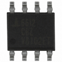
ISL6612CBZ Intersil, ISL6612CBZ Datasheet - Page 9

ISL6612CBZ
Manufacturer Part Number
ISL6612CBZ
Description
IC DRVR MOSF SYNC BUCK OTP 8SOIC
Manufacturer
Intersil
Datasheet
1.ISL6612CBZ.pdf
(12 pages)
Specifications of ISL6612CBZ
Configuration
High and Low Side, Synchronous
Input Type
PWM
Delay Time
10.0ns
Current - Peak
1.25A
Number Of Configurations
1
Number Of Outputs
2
High Side Voltage - Max (bootstrap)
36V
Voltage - Supply
10.8 V ~ 13.2 V
Operating Temperature
0°C ~ 85°C
Mounting Type
Surface Mount
Package / Case
8-SOIC (3.9mm Width)
Lead Free Status / RoHS Status
Lead free / RoHS Compliant
Available stocks
Company
Part Number
Manufacturer
Quantity
Price
Part Number:
ISL6612CBZ
Manufacturer:
INTERSIZ
Quantity:
20 000
Part Number:
ISL6612CBZ-T
Manufacturer:
INTERSIL
Quantity:
20 000
Part Number:
ISL6612CBZA
Manufacturer:
ISL
Quantity:
20 000
Company:
Part Number:
ISL6612CBZA-T
Manufacturer:
ST
Quantity:
24 000
Part Number:
ISL6612CBZA-T
Manufacturer:
INTERSIL
Quantity:
20 000
P
P
P
R
is approximately 800mW at room temperature, while the
power dissipation capacity in the EPSOIC and DFN
packages, with an exposed heat escape pad, is more than 2W
and 1.5W, respectively. Both EPSOIC and DFN packages are
more suitable for high frequency applications. See “Layout
Considerations” on page 9 for thermal transfer improvement
suggestions. When designing the driver into an application, it
is recommended that the following calculation is used to
ensure safe operation at the desired frequency for the
selected MOSFETs. The total gate drive power losses due to
the gate charge of MOSFETs and the driver’s internal circuitry
and their corresponding average driver current can be
estimated using Equation 2 and Equation 3, respectively,
where the gate charge (Q
particular gate to source voltage (V
corresponding MOSFET data sheet; I
quiescent current with no load at both drive outputs; N
and N
respectively; UVCC and LVCC are the drive voltages for
both upper and lower FETs, respectively. The I
product is the quiescent power of the driver without
capacitive load and is typically 116mW at 300kHz.
The total gate drive power losses are dissipated among the
resistive components along the transition path. The drive
resistance dissipates a portion of the total gate drive power
losses, the rest will be dissipated by the external gate
resistors (R
and R
upper and lower gate drives turn-on transition path. The
power dissipation on the driver can be roughly estimated as:
DR
DR_UP
DR_LOW
P
EXT1
I
DR
Qg_TOT
=
P
P
=
GI2
Qg_Q1
Qg_Q2
Q2
P
=
⎛
⎜
⎝
DR_UP
=
Q
----------------------------------------------------- -
R
=
) of MOSFETs. Figures 3 and 4 show the typical
are number of upper and lower MOSFETs,
⎛
⎜
⎝
=
G1
G1
--------------------------------------
R
G1
⎛
⎜
⎝
P
HI1
--------------------------------------
R
=
•
+
=
Qg_Q1
HI2
UVCC N
+
and R
R
-------------
V
R
N
Q
-------------------------------------- - F
Q
------------------------------------- - F
+
P
GI1
GS1
HI1
Q1
R
G1
G2
R
+
DR_LOW
HI2
EXT1
R
V
V
•
•
+
GS2
EXT2
G2
GS1
•
UVCC
LVCC
P
Qg_Q2
) and the internal gate resistors (R
Q1
+
G1
+
+
--------------------------------------- -
R
+
2
I
LO1
--------------------------------------- -
R
2
Q
R
•
Q
---------------------------------------------------- -
and Q
•
LO2
EXT2
+
•
9
R
G2
I
VCC
SW
LO1
+
Q
SW
R
R
+
LO2
•
•
LVCC N
EXT1
R
•
VCC
V
GS1
G2
=
•
EXT2
N
GS2
N
R
Q
Q2
) is defined at a
Q1
G2
and V
⎞
⎟
⎠
is the driver’s total
•
⎞
⎟
⎠
•
+
P
---------------------
•
R
-------------
Qg_Q1
N
Q2
P
---------------------
GS2
GI2
Q2
Qg_Q2
2
⎞
⎟
⎠
Q*
2
•
VCC
) in the
F
SW
ISL6612, ISL6613
(EQ. 4)
(EQ. 2)
(EQ. 3)
+
Q1
I
Q
GI1
Layout Considerations
For heat spreading, place copper underneath the IC whether
it has an exposed pad or not. The copper area can be
extended beyond the bottom area of the IC and/or
connected to buried copper plane(s) with thermal vias. This
combination of vias for vertical heat escape, extended
copper plane, and buried planes for heat spreading allows
the IC to achieve its full thermal potential.
Place each channel power component as close to each
other as possible to reduce PCB copper losses and PCB
parasitics: shortest distance between DRAINs of upper FETs
and SOURCEs of lower FETs; shortest distance between
DRAINs of lower FETs and the power ground. Thus, smaller
amplitudes of positive and negative ringing are on the
switching edges of the PHASE node. However, some space
in between the power components is required for good
airflow. The traces from the drivers to the FETs should be
kept short and wide to reduce the inductance of the traces
and to promote clean drive signals.
FIGURE 4. TYPICAL LOWER-GATE DRIVE TURN-ON PATH
FIGURE 3. TYPICAL UPPER-GATE DRIVE TURN-ON PATH
UVCC
LVCC
PHASE
R
R
BOOT
LO2
R
HI2
R
LO1
HI1
R
G2
R
G
G1
G
R
C
GI2
R
GD
C
C
GI1
GD
GS
C
GS
S
S
D
D
Q
June 15, 2010
C
2
Q
DS
C
1
FN9153.9
DS


