IRS21844SPBF International Rectifier, IRS21844SPBF Datasheet
IRS21844SPBF
Specifications of IRS21844SPBF


Related parts for IRS21844SPBF

IRS21844SPBF Summary of contents
Page 1
Features · Floating channel designed for bootstrap operation · Fully operational to +600 V · Tolerant to negative transient voltage, dV/dt immune · Gate drive supply range from · Undervoltage lockout for both channels · ...
Page 2
Absolute Maximum Ratings Absolute maximum ratings indicate sustained limits beyond which damage to the device may occur. All voltage parameters are absolute voltages referenced to COM. The thermal resistance and power dissipation ratings are measured under board mounted and still ...
Page 3
Recommended Operating Conditions The input/output logic timing diagram is shown in Fig. 1. For proper operation the device should be used within the recommended conditions. The V and V S Symbol V High-side floating supply absolute voltage B V High-side ...
Page 4
Static Electrical Characteristics COM, DT= V BIAS parameters are referenced to V /COM and are applicable to the respective input leads: IN and SD. The V SS ...
Page 5
Functional Block Diagrams 2184 IN DEADTIME +5V SD 21844 IN DEADTIME DT +5V SD VSS www.irf.com IRS2184/IRS21844(S)PbF PULSE HV FILTER LEVEL SHIFTER VSS/COM LEVEL PULSE SHIFT GENERATOR VSS/COM LEVEL DELAY SHIFT HV LEVEL SHIFTER VSS/COM LEVEL PULSE SHIFT GENERATOR VSS/COM ...
Page 6
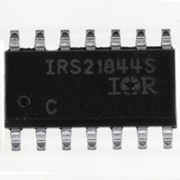
... Low-side and logic fixed supply CC LO Low-side gate drive output COM Low-side return Lead Assignments COM 8-Lead PDIP IRS2184PbF VSS COM 14-Lead PDIP IRS21844PbF www.irf.com IRS2184/IRS21844(S)PbF COM for IRS2184 and VSS for IRS21844) 4 only only COM 8-Lead SOIC IRS2184SPbF VSS COM 14-Lead SOIC IRS21844SPbF 6 ...
Page 7
Figure 1. Input/Output Timing Diagram SD 50 90% LO Figure 3. Shutdown Waveform Definitions Figure 5. Delay Matching Waveform Definitions www.irf.com IRS2184/IRS21844(S)PbF IN (LO) 50% IN (HO Figure 2. ...
Page 8
Tolerant to Negative V Transients S A common problem in today’s high-power switching converters is the transient response of the switch node’s voltage as the power switches transition on and off quickly while carrying a large current. A typical half ...
Page 9
... International Rectifier’s HVICs have been designed for the robustness required in many of today’s demanding applications. An indication of the IRS2184(4)’s robustness can be seen in Figure 14, where there ...
Page 10
Figure 12: Negative V Even though the IRS2184(4) has been shown able to handle these large negative V is highly recommended that the circuit designer always limit the negative V by careful PCB layout and component use. www.irf.com IRS2184/IRS21844(S)PbF transient ...
Page 11
Max. 200 Typ. 100 0 -50 - Temperature ( C) Figure 13A. Turn-On Propagation Delay Time vs. Temperature 700 600 500 400 Max. 300 Typ. 200 100 -50 - ...
Page 12
Max. 200 Typ. 100 0 -50 - Temperature ( Figure 15A. SD Propagation Delay vs. Temperature 120 100 Max Typ -50 - Temperature ( Figure 16A. ...
Page 13
Max. Typ 20 0 -50 - Temperature ( C) Figure 17A. Turn-Off Fall Time vs. Temperature 1100 900 700 Max. 500 Typ. Min. 300 100 -50 - Temperature ( Figure ...
Page 14
Figure 18C. Deadtime vs Max Supply Voltage (V) BAIS Figure ...
Page 15
Max Supply Voltage (V) Figure 20B. Logic “0” Input Voltage vs. Supply Voltage Max Supply Voltage (V) CC ...
Page 16
Max Supply Voltage (V) Figure 22B. SD Input Negative Going Threshold vs. Supply Voltage 5.0 4.0 3.0 2.0 Max 1.0 0 Supply Voltage (V) BIAS ...
Page 17
Max. 0.2 0.1 0 Supply Voltage (V) Figure 24B. Low Level Output vs. Supply Voltage 500 400 300 200 100 Max. 0 100 200 300 400 V Boost Voltage (V) B Figure 25B. ...
Page 18
V Floating Supply Voltage (V) BS Figure 26B. V Supply Current BS vs. V Supply Voltage Supply Voltage ...
Page 19
Max. 40 Typ Supply Voltage (V) Figure 28B. Logic “1” Input Bias Current vs. Supply Voltage 6 5 Max Supply Voltage ...
Page 20
Max. 9 Typ -50 - Temperature ( Figure 31. V and V Undervoltage Threshold (-) CC BS vs. Temperature Typ ...
Page 21
Typ Supply Voltage (V) Figure 33B. Output Sink Current vs. Supply Voltage 140 120 100 Frequency (kHz) Figure 35. IRS2184 vs. ...
Page 22
Frequency (kHz) Figure 37. IRS2184 vs. Frequency (IRFBC50 10W, V gate cc 140 120 100 Frequency (kHz) Figure 39. IRS21844 vs. Frequency (IRFBC30), ...
Page 23
Frequency (kHz) Figure 41. IRS21844 vs. Frequency (IRFBC50 10W, V gate cc 140 120 100 Frequency (kHz) Figure 43. IRS2184s vs. Frequency (IRFBC30), ...
Page 24
Frequency (kHz) Figure 45. IRS2184s vs. Frequency (IRFBC50 10W, V gate cc 140 120 100 Frequency (kHz) Figure 47. IRS21844s vs. Frequency (IRFBC30), ...
Page 25
Figure 49. IRS21844s vs. Frequency (IRFBC50), www.irf.com IRS2184/IRS21844(S)PbF 140 120 100 100 Frequency (kHz 10W 15V gate cc 140v 70v 0v 1000 25 ...
Page 26
Cast Outlines 0.25 [.010 0.25 [.010 NOTES: 1. DIMENSIONING & TOLERANCING PER ASME Y14.5M-1994. 2. CONTROLLING ...
Page 27
IRS2184/IRS21844(S)PbF 14-Lead PDIP 14-Lead SOIC (narrow body) 01-6010 01-3002 03 (MS-001AC) 01-6019 01-3063 00 (MS-012AB) 27 ...
Page 28
Tape & Reel 8-lead SOIC NTROLLING D IM ENSION ...
Page 29
Tape & Reel 14-lead SOIC NTROLLING D IM ENSION ...
Page 30
... Assembly site code Per SCOP 200-002 ORDER INFORMATION 14-Lead PDIP IR2S1844PbF 14-Lead SOIC IRS21844SPbF 14-Lead SOIC Tape & Reel IRS21844STRPbF This product has been designed and qualified for the industrial level. Qualification standards can be found at www.irf.com Data and specifications subject to change without notice. 12/1/2006 ...