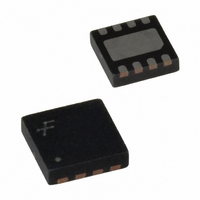
FAN5009MPX Fairchild Semiconductor, FAN5009MPX Datasheet

FAN5009MPX
Specifications of FAN5009MPX
Related parts for FAN5009MPX
FAN5009MPX Summary of contents
Page 1
... On Low Battery Detect In Low Battery Detect Out ©2005 Fairchild Semiconductor Corporation FAN4855 Rev. 1.0.1 General Description The FAN4855 is a low power boost regulator designed for low voltage conversion in 2-cell battery powered systems such as digital cameras, cell phones and PDAs. The converter starts-up at 1.3V and operates after the start at an input voltage as low as 1V ...
Page 2
Pin Configuration Pin Description Pin Name 1 V Battery Input Voltage. Supplies the IC during start-up. After the output is running, the IC draws IN power from V 2 SHDN Shut Down. Pulling this pin low shuts down the regulator, ...
Page 3
Recommended Operating Conditions Parameter Ambient Temperature Range V Operating Range IN V Operating Range OUT Electrical Characteristics Unless otherwise specified 1. +25°C A Parameter Start Up Voltage Operating Voltage Output Voltage Output ...
Page 4
VIN 2 1 1.6V to 3.0V R1 750K SHDN 2 1 Reset 47µF R2 240K Ext Pull GND 2 1 FAN4855 Rev. 1.0.1 10uH U1 FAN4855 JP2 1 8 Vin Gnd 2 7 ...
Page 5
Typical Operating Characteristics Load Current vs. Start-Up Voltage (Resistive Load) 600 500 V = 3.3V OUT 400 300 200 100 0 1.5 2 2.5 Input Voltage, V Efficiency vs. Load Current Vout = 5V 100.0 Vin=3V 90.0 80.0 Vin=2.0V Vin=1.5V ...
Page 6
Typical Operating Characteristics No Load Supply Current vs. Input Voltage 1000 “ON” OUT 100 V = 3.3V OUT 10 “OFF” Input Voltage (V) FAN4855 Rev. 1.0 10µ 47µF, ...
Page 7
Typical Operating Characteristics Line Transient Response @100mA Load Load Transient Response Heavy-Load Switching Waveforms FAN4855 Rev. 1.0.1 (Continued) Inductor Current and Switching Node Voltage OUT 7 Exiting Shutdown V OUT V SHDN Load Transient Response ...
Page 8
Block Diagram LBO 4 LBI 3 – 0.39V V V OUT IN Start-Up 1 Minimum Off-Time Logic Variable On-Time One Shot I SHDN LIMIT Functional Description Boost Regulator FAN4855 is an adjustable boost regulator that combines variable ON ...
Page 9
The synchronous rectifier significantly improves effi- ciency without the addition of an external component, so that conversion efficiency can be as high as 94% over a large load range, as shown in the Typical Operating Characteristics. Even at light loads, ...
Page 10
Layout and Grounding Considerations Careful design of printed circuit board is recommended since high frequency switching and high peak currents are present in DC/DC converters applications. A general rule is to place the converter circuitry well away from any sensitive ...
Page 11
Mechanical Dimensions Package: T08, 8-Pin TSSOP 0.113 - 0.123 (2.87 - 3.12) 8 PIN 0.026 BSC (0.65 BSC) 0.008 - 0.012 0.033 - 0.037 (0.20 - 0.30) (0.84 - 0.94) FAN4855 Rev. 1.0.1 0.169 - 0.177 0.246 ...
Page 12
... The following are registered and unregistered trademarks Fairchild Semiconductor owns or is authorized to use and is not intended exhaustive list of all such trademarks. FAST ACEx™ ActiveArray™ FASTr™ Bottomless™ FPS™ Build it Now™ FRFET™ CoolFET™ GlobalOptoisolator™ ...


