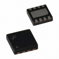
FAN5009MPX Fairchild Semiconductor, FAN5009MPX Datasheet - Page 2
FAN5009MPX
Manufacturer Part Number
FAN5009MPX
Description
IC DRIVER MOSFET DUAL 12V 8MLP
Manufacturer
Fairchild Semiconductor
Type
High Side/Low Sider
Specifications of FAN5009MPX
Configuration
High and Low Side, Synchronous
Input Type
Inverting and Non-Inverting
Delay Time
50ns
Number Of Configurations
1
Number Of Outputs
2
High Side Voltage - Max (bootstrap)
15V
Voltage - Supply
6.4 V ~ 13.5 V
Operating Temperature
0°C ~ 85°C
Mounting Type
Surface Mount
Package / Case
8-MLP
Supply Voltage (min)
10 V
Supply Current
8 mA
Maximum Power Dissipation
715 mW
Maximum Operating Temperature
+ 85 C
Mounting Style
SMD/SMT
Minimum Operating Temperature
0 C
Number Of Drivers
2
Lead Free Status / RoHS Status
Lead free / RoHS Compliant
Current - Peak
-
Lead Free Status / Rohs Status
Lead free / RoHS Compliant


FAN4855 Rev. 1.0.1
Pin Configuration
Pin Description
Absolute Maximum Ratings
Absolute Maximum Ratings are those values, beyond which the device could be permanently damaged. Absolute max-
imum ratings are stress ratings only and functional device operation is not implied.
V
Switch Voltage (V
Voltage on any other Pin
Peak Switch Current (Ipeak)
Output Current (I
Continuous Power Dissipation
Thermal Resistance (θ
Junction Temperature
Storage Temperature Range
Lead Temperature (soldering, 10s)
Parameter
Pin
IN
1
2
3
4
5
6
7
8
, V
OUT
Name
SHDN
V
GND
LBO
Voltages (Relative to GND)
LBI
FB
V
OUT
V
IN
L
OUT
L
Battery Input Voltage. Supplies the IC during start-up. After the output is running, the IC draws
power from V
Shut Down. Pulling this pin low shuts down the regulator, isolating the load from the input.
Low-Battery Input. Pulling this pin below 0.39V causes the LBO pin to go low.
Low-Battery Output. This pin provides an active low signal to alert the user when the LBI voltage
falls below its targeted value. The open-drain output can be used to reset a microcontroller.
Feedback Input. For setting the output voltage. Connect this pin to the resistor divider.
Boost regulator output. Output voltage can be set to be in the 3 to 5V range. Startup at moderate
load is achievable at input voltages around 1.35V.
Boost inductor connection. Connect an inductor between this pin and V
output supply, this pin pulls low, charging the inductor, then shuts off dumping the energy through
the synchronous rectifier to the output.
Ground of the IC.
to GND)
)
JA
)
OUT
.
SHDN
LB0
LBI
V
IN
1
2
3
4
8-Pin TSSOP
TOP VIEW
2
Function
8
7
6
5
Min.
-0.3
-0.3
-0.3
-65
GND
V
V
FB
L
OUT
— Internally Limited —
V
V
OUT
OUT
Max.
500
124
150
525
150
300
6.5
+ 0.3
+ 0.3
IN
. When servicing the
www.fairchildsemi.com
Units
°C/W
mW
mA
°C
°C
°C
V
V
V
Related parts for FAN5009MPX
Image
Part Number
Description
Manufacturer
Datasheet
Request
R

Part Number:
Description:
Dual Bootstrapped 12V MOSFET Driver
Manufacturer:
Fairchild Semiconductor
Datasheet:
Part Number:
Description:
Fairchild Semiconductor [IGBT MODULE]
Manufacturer:
Fairchild Semiconductor
Datasheet:

Part Number:
Description:
Discrete Semiconductor Modules
Manufacturer:
Fairchild Semiconductor
Part Number:
Description:
Discrete Semiconductor Modules
Manufacturer:
Fairchild Semiconductor
Part Number:
Description:
This N-Channel MOSFET is produced using Fairchild Semiconductor’s advanced Power Trench® process
Manufacturer:
Fairchild Semiconductor
Datasheet:
Part Number:
Description:
This N-Channel MOSFET is produced using Fairchild Semiconductor’s advanced Power Trench® process
Manufacturer:
Fairchild Semiconductor
Datasheet:
Part Number:
Description:
This N-Channel MOSFET is produced using Fairchild Semiconductor’s advanced PowerTrench® process
Manufacturer:
Fairchild Semiconductor
Datasheet:
Part Number:
Description:
This N-Channel MOSFET is produced using Fairchild Semiconductor’s advanced PowerTrench® process
Manufacturer:
Fairchild Semiconductor
Datasheet:
Part Number:
Description:
This N-Channel MOSFET is produced using Fairchild Semiconductor’s advanced Power Trench® process
Manufacturer:
Fairchild Semiconductor
Datasheet:
Part Number:
Description:
This N-Channel logic Level MOSFETs are produced using Fairchild Semiconductor‘s advanced Power Trench® process that has been special tailored to minimize the on-state resistance and yet maintain superior switching performance
Manufacturer:
Fairchild Semiconductor
Datasheet:
Part Number:
Description:
This N-Channel MOSFET is produced using Fairchild Semiconductor’s advanced Power Trench® process
Manufacturer:
Fairchild Semiconductor
Datasheet:
Part Number:
Description:
This N-Channel SyncFET™ is produced using Fairchild Semiconductor’s advanced PowerTrench® process
Manufacturer:
Fairchild Semiconductor
Datasheet:
Part Number:
Description:
This N-Channel SyncFET™ is produced using Fairchild Semiconductor’s advanced PowerTrench® process
Manufacturer:
Fairchild Semiconductor
Datasheet:
Part Number:
Description:
This N-Channel SyncFET™ is produced using Fairchild Semiconductor’s advanced PowerTrench® process
Manufacturer:
Fairchild Semiconductor
Datasheet:
Part Number:
Description:
This N-Channel logic Level MOSFETs are produced using Fairchild Semiconductor‘s advanced Power Trench® process that has been special tailored to minimize the on-state resistance and yet maintain superior switching performance
Manufacturer:
Fairchild Semiconductor
Datasheet: