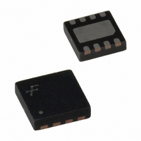
FAN5009MPX Fairchild Semiconductor, FAN5009MPX Datasheet - Page 9

FAN5009MPX
Manufacturer Part Number
FAN5009MPX
Description
IC DRIVER MOSFET DUAL 12V 8MLP
Manufacturer
Fairchild Semiconductor
Type
High Side/Low Sider
Specifications of FAN5009MPX
Configuration
High and Low Side, Synchronous
Input Type
Inverting and Non-Inverting
Delay Time
50ns
Number Of Configurations
1
Number Of Outputs
2
High Side Voltage - Max (bootstrap)
15V
Voltage - Supply
6.4 V ~ 13.5 V
Operating Temperature
0°C ~ 85°C
Mounting Type
Surface Mount
Package / Case
8-MLP
Supply Voltage (min)
10 V
Supply Current
8 mA
Maximum Power Dissipation
715 mW
Maximum Operating Temperature
+ 85 C
Mounting Style
SMD/SMT
Minimum Operating Temperature
0 C
Number Of Drivers
2
Lead Free Status / RoHS Status
Lead free / RoHS Compliant
Current - Peak
-
Lead Free Status / Rohs Status
Lead free / RoHS Compliant
FAN4855 Rev. 1.0.1
The synchronous rectifier significantly improves effi-
ciency without the addition of an external component, so
that conversion efficiency can be as high as 94% over a
large load range, as shown in the Typical Operating
Characteristics. Even at light loads, the efficiency stays
high because the switching losses of the converter are
minimized by reducing the switching frequency.
Error Detection Comparator (LBI – LBO)
An additional comparator A3 is provided to detect low V
or any other error conditions that is important to the user.
The non-inverting input of the comparator is internally
connected to a reference threshold voltage V
inverting input is connected to the LBI pin. The output of
the low battery comparator is a simple open-drain output
that goes active low if the battery voltage drops below
the programmed threshold voltage on LBI. The output
requires a pull-up resistor having a recommended value
of 100 kΩ, should be connected only to V
The low-battery detector circuit is typically used to super-
vise the battery voltage and to generate an error flag or a
RESET command when the battery voltage drops below
a user-set threshold voltage. The function is active only
when the device is enabled. When the device is disabled,
the LBO-pin is high impedance.
Shutdown
The device enters shutdown when V
mately less than 0.5V
stops switching, all internal control circuitry including the
low-battery comparator is switched off and the load is
disconnected from the input. The output voltage may
drop below the input voltage during shutdown. The typi-
cal dependence shutdown voltage versus input voltage
and the timing process of the exiting shutdown are
shown on the Diagrams. For normal operation V
should be driven up 0.8V
Application Information
Selecting the Output Voltage
The output voltage V
choosing resistors R4 and R5 of the divider in the feed-
back circuit (see Test Circuit). The value of the R5 is rec-
ommended to be less than 270k. R4 can be calculated
using the following equation:
R4 = R5[(V
where V
Setting the LBI Threshold of Low-Battery
Detector Circuit
The LBO-pin goes active low when the voltage on the
LBI-pin decreases below the set threshold typical voltage
of 390 mV, which is set by to the internal reference volt-
age.
REF
OUT
= 1.24V
/V
REF
) – 1]
OUT
IN
. During shutdown the regulator
IN
can be adjusted from 3V to 5V,
or connected to the V
SHDN
OUT
.
th
is approxi-
while the
IN
.
SHDN
IN
9
The battery voltage, at which the detection circuit
switches, can be programmed with a resistive divider
connected to the LBI-pin. The resistive divider scales
down the battery voltage to a voltage level of tenths of
volt, which is then compared to the LBI threshold voltage.
The LBI-pin has a built-in hysteresis of 25 mV. The resis-
tor values R1 and R2 can be calculated using the follow-
ing equation:
V
The value of R2 should be 270k or less to minimize bias
current errors. R1 is then found by rearranging the equa-
tion:
R1 = R2 x (V
If the low-battery detection circuit is not used, the LBI-pin
should be connected to GND (or to V
can be left unconnected or tied to GND. Do not let the
LBI-pin float.
Component Selection
Input and Output Capacitors Selection
For common general purpose applications, 47µF tanta-
lum capacitors are recommended. Ceramic capacitors
are recommended at input only; if connected at the out-
put they cannot improve significantly the voltage ripple.
More effective in reducing the output ripple at light load is
to connect a small capacitor of 18 to 100pF between
V
Table 1. Recommended capacitors
Inductor Selection
The inductor parameters directly influencing the device
performance are the saturation current and the DC resis-
tance. The FAN4855 operates with a typical inductance
of 10µH. The lower the resistance, the higher the effi-
ciency. The saturation current should be rated higher
than 0.8A, which is the typical threshold to switch off the
N-channel power FET.
Table 2. Recommended Inductors
Vendor
MuRata
AVX
Sprague
Kemet
Supplier
MuRata
Coilcraft
Coiltronics
Sumida
OUT
IN_MIN
and FB pin.
= 0.39 x (R1+R2)/R2
IN_MIN
Manufacturer Part Number
LQ66C100M4
DT1608C-103
UP1B100
CDR63B-100
/0.39 – 1)
Description
X5R Ceramic
TAJ,TPS series tantalum
595D series tantalum
T494 series tantalum
IN
) and the LBO-pin
www.fairchildsemi.com


