IXDN404SI IXYS, IXDN404SI Datasheet
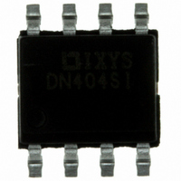
IC MOSFET DRVR LS 4A DUAL 8-SOIC

IXDN404SI

Manufacturer Part Number
IXDN404SI
Description
IC MOSFET DRVR LS 4A DUAL 8-SOIC
Manufacturer
IXYS
Type
Low Side Gate Driverr
Datasheet

Specifications of IXDN404SI

Configuration
Low-Side
Input Type
Non-Inverting
Delay Time
36ns
Current - Peak
4A
Number Of Configurations
2
Number Of Outputs
2
Voltage - Supply
4.5 V ~ 35 V
Operating Temperature
-55°C ~ 125°C
Mounting Type
Surface Mount
Package / Case
8-SOIC
Number Of Drivers
2
Driver Configuration
Non-Inverting
Driver Type
Low Side
Input Logic Level
CMOS/TTL
Rise Time
18ns
Fall Time
17ns
Operating Supply Voltage (max)
35V
Peak Output Current
4mA
Output Resistance
1.5/2Ohm
Operating Supply Voltage (min)
4.5V
Operating Supply Voltage (typ)
18V
Turn Off Delay Time
39fs
Turn On Delay Time (max)
40ps
Operating Temp Range
-55C to 125C
Operating Temperature Classification
Military
Mounting
Surface Mount
Pin Count
8
Package Type
SOIC
Supply Voltage (min)
4.5 V
Supply Current
3 mA
Maximum Operating Temperature
+ 125 C
Mounting Style
SMD/SMT
Minimum Operating Temperature
- 55 C
Output Current
4 A
For Use With
EVDN404 - BOARD EVALUATION IXDN404
Lead Free Status / RoHS Status
Lead free / RoHS Compliant
High Side Voltage - Max (bootstrap)
-
Lead Free Status / Rohs Status
Compliant

Available stocks

Company
Part Number
Manufacturer
Quantity
Price
Part Number:
IXDN404SI
Manufacturer:
2002+
Quantity:
6 221
Part Number:
IXDN404SI
Manufacturer:
IXYS/艾赛斯
Quantity:
20 000
Part Number:
IXDN404SI-16
Manufacturer:
IXYS
Quantity:
4 899
Part Number:
IXDN404SIA
Manufacturer:
IXYS/艾赛斯
Quantity:
20 000
Part Number:
IXDN404SIA-16
Manufacturer:
IXYS
Quantity:
5 787
Features
• Built using the advantages and compatibility
• Latch-Up Protected
• High Peak Output Current: 4A Peak
• Wide Operating Range: 4.5V to 35V
• High Capacitive Load
• Matched Rise And Fall Times
• Low Propagation Delay Time
• Low Output Impedance
• Low Supply Current
• Two Drivers in Single Chip
Applications
• Driving MOSFETs and IGBTs
• Motor Controls
• Line Drivers
• Pulse Generators
• Local Power ON/OFF Switch
• Switch Mode Power Supplies (SMPS)
• DC to DC Converters
• Pulse Transformer Driver
• Class D Switching Amplifiers
• Limiting di/dt Under Short Circuit
Copyright © IXYS CORPORATION 2004
of CMOS and IXYS HDMOS
Drive Capability: 1800pF in <15ns
Ordering Information
NOTE: Mounting or solder tabs on all packages are connected to ground
Part Number
IXDN404PI
IXDN404SI
IXDN404SIA
IXDN404SI-16
IXDN404SIA-16
IXDI404PI
IXDI404SI
IXDI404SIA
IXDI404SI-16
IXDI404SIA-16
IXDF404PI
IXDF404SI
IXDF404SIA
IXDF404SI-16
IXDF404SIA-16
Package Type
8-Pin PDIP
8-Pin SOIC with Grounded Metal Back
8-Pin SOIC
16-Pin SOIC with Grounded Metal Back
16-Pin SOIC
8-Pin PDIP
8-Pin SOIC with Grounded Metal Back
8-Pin SOIC
16-Pin SOIC with Grounded Metal Back
16-Pin SOIC
8-Pin PDIP
8-Pin SOIC with Grounded Metal Back
8-Pin SOIC
16-Pin SOIC with Grounded Metal Back
16-Pin SOIC
TM
4 Ampere Dual Low-Side Ultrafast MOSFET Drivers
IXDN404 / IXDI404 / IXDF404
processes
General Description
The IXDN404/IXDI404/IXDF404 is comprised of two 4 Ampere
CMOS high speed MOSFET drivers. Each output can source
and sink 4A of peak current while producing voltage rise and
fall times of less than 15ns to drive the latest IXYS MOSFETs
and IGBT's. The input of the driver is compatible with TTL or
CMOS and is fully immune to latch up over the entire operating
range. A patent-pending circuit virtually eliminates CMOS
power supply cross conduction and current shoot-through.
Improved speed and drive capabilities are further enhanced by
very low, matched rise and fall times.
The IXDN404 is configured as a dual non-inverting gate driver,
the IXDI404 is a dual inverting gate driver, and the IXDF404 is a
dual inverting + non-inverting gate driver.
The IXDN404/IXDI404/IXDF404 family are available in the
standard 8 pin P-DIP (PI), SOIC-8 (SIA) and SOIC-16 (SIA-16)
packages. For enhanced thermal performance, the SOP-8 and
SOP-16 are also available in a package with an exposed
grounded metal back as the SI and SI-16 repectively.
First Release
Temp. Range
-55°C to
-55°C to
-55°C to
+125°C
+125°C
+125°C
Configuration
Dual Inverting
Non Inverting
Inverting +
Dual Non
Inverting
DS99018D(11/10)

Related parts for IXDN404SI

IXDN404SI Summary of contents

Page 1

... Package Type IXDN404PI 8-Pin PDIP IXDN404SI 8-Pin SOIC with Grounded Metal Back IXDN404SIA 8-Pin SOIC IXDN404SI-16 16-Pin SOIC with Grounded Metal Back IXDN404SIA-16 16-Pin SOIC IXDI404PI 8-Pin PDIP IXDI404SI 8-Pin SOIC with Grounded Metal Back IXDI404SIA 8-Pin SOIC IXDI404SI-16 16-Pin SOIC with Grounded Metal Back ...

Page 2

Figure 1 - IXDN404 Dual 4A Non-Inverting Gate Driver Functional Block Diagram GND Figure 2 - IXDI404 Dual Inverting 4A Gate Driver Functional Block Diagram GND Figure 3 - IXDF404 Inverting + ...

Page 3

Absolute Maximum Ratings Parameter Value Supply Voltage 40V All Other Pins -0. 0.3V Junction Temperature 150 o C Storage Temperature - 150 o C Soldering Lead Temperature 300 o C (10 seconds maximum) ...

Page 4

Electrical Characteristics Unless otherwise noted, temperature over -55 All voltage measurements with respect to GND. Device configured as described in Test Conditions. All specifications are for one channel. Symbol Parameter V High input voltage IH V Low input voltage IL ...

Page 5

Pin Description SYMBOL FUNCTION Channel Input GND Ground Channel Input OUT B B Channel Output VCC Supply Voltage OUT A A Channel Output CAUTION: These devices are sensitive to electrostatic discharge; follow proper ESD ...

Page 6

Typical Performance Characteristics Fig. 5 Rise Times vs. Supply Voltage Supply Voltage (V) Fig. 7 Output Rise Tim es vs. Load Capacitance ...

Page 7

Supply Current vs. Load Capacitance Fig. 11 Vcc = 8V 100 100 1000 Load Capacitance (pF) Supply Current vs. Load Capacitance Fig. 13 Vcc = 12V 100 2 MHz 90 ...

Page 8

Fig. 17 Supply Current vs. Load Capacitance Vcc = 35V 100 MHz 70 1 MHz 100 1000 Load Capacitance (pF) Propagation Delay vs. Supply Voltage Fig 1800pF ...

Page 9

Fig. 23 High State Ouput Resistance vs. Supply Voltage Supply Voltage (V) Fig vs. P Channel Output Current -10 -12 5 ...

Page 10

... Pin SOIC IXDN404SI-16 Supply Bypassing, Grounding Practices And Output Lead inductance When designing a circuit to drive a high speed MOSFET utilizing the IXDN404/IXDI404/IXDF404 very important to observe certain design criteria in order to optimize performance of the driver. Particular attention needs to be paid to Supply Bypassing, Grounding, and minimizing the Output Lead Inductance ...

Page 11

... Dimenional Outline: IXDD404PI Dimenional Outlines: IXDD404SI-CT and IXDD404SIA Dimenional Outlines: IXDD404SI-16CT and IXDD404SIA-16 IXDN404 / IXDI404 / IXDF404 IXYS Corporation 3540 Bassett St; Santa Clara, CA 95054 Tel: 408-982-0700; Fax: 408-496-0670 e-mail: sales@ixys.net IXYS Semiconductor GmbH Edisonstrasse15 ; D-68623; Lampertheim Tel: +49-6206-503-0; Fax: +49-6206-503627 e-mail: marcom@ixys.de 11 ...

Related keywords