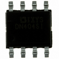
IXDN404SI IXYS, IXDN404SI Datasheet - Page 3

IXDN404SI
Manufacturer Part Number
IXDN404SI
Description
IC MOSFET DRVR LS 4A DUAL 8-SOIC
Manufacturer
IXYS
Type
Low Side Gate Driverr
Datasheet
1.IXDF404SI.pdf
(11 pages)
Specifications of IXDN404SI
Configuration
Low-Side
Input Type
Non-Inverting
Delay Time
36ns
Current - Peak
4A
Number Of Configurations
2
Number Of Outputs
2
Voltage - Supply
4.5 V ~ 35 V
Operating Temperature
-55°C ~ 125°C
Mounting Type
Surface Mount
Package / Case
8-SOIC
Number Of Drivers
2
Driver Configuration
Non-Inverting
Driver Type
Low Side
Input Logic Level
CMOS/TTL
Rise Time
18ns
Fall Time
17ns
Operating Supply Voltage (max)
35V
Peak Output Current
4mA
Output Resistance
1.5/2Ohm
Operating Supply Voltage (min)
4.5V
Operating Supply Voltage (typ)
18V
Turn Off Delay Time
39fs
Turn On Delay Time (max)
40ps
Operating Temp Range
-55C to 125C
Operating Temperature Classification
Military
Mounting
Surface Mount
Pin Count
8
Package Type
SOIC
Supply Voltage (min)
4.5 V
Supply Current
3 mA
Maximum Operating Temperature
+ 125 C
Mounting Style
SMD/SMT
Minimum Operating Temperature
- 55 C
Output Current
4 A
For Use With
EVDN404 - BOARD EVALUATION IXDN404
Lead Free Status / RoHS Status
Lead free / RoHS Compliant
High Side Voltage - Max (bootstrap)
-
Lead Free Status / Rohs Status
Compliant
Available stocks
Company
Part Number
Manufacturer
Quantity
Price
Company:
Part Number:
IXDN404SI
Manufacturer:
2002+
Quantity:
6 221
Part Number:
IXDN404SI
Manufacturer:
IXYS/艾赛斯
Quantity:
20 000
Company:
Part Number:
IXDN404SI-16
Manufacturer:
IXYS
Quantity:
4 899
Part Number:
IXDN404SIA
Manufacturer:
IXYS/艾赛斯
Quantity:
20 000
Company:
Part Number:
IXDN404SIA-16
Manufacturer:
IXYS
Quantity:
5 787
Thermal Resistance (Junction to Case)
Electrical Characteristics
Absolute Maximum Ratings
Specifications Subject To Change Without Notice
Note 1: Operating the device beyond parameters with listed “Absolute Maximum Ratings” may cause permanent
damage to the device. Typical values indicate conditions for which the device is intended to be functional, but do not
guarantee specific performance limits. The guaranteed specifications apply only for the test conditions listed.
Exposure to absolute maximum rated conditions for extended periods may affect device reliability.
Unless otherwise noted, T
All voltage measurements with respect to GND. Device configured as described in Test Conditions. All specifications are for one channel.
Parameter
Supply Voltage
All Other Pins
Junction Temperature
Storage Temperature
Soldering Lead Temperature
(10 seconds maximum)
Symbol
V
V
V
I
V
V
R
R
I
I
t
t
t
t
V
I
8 Pin SOIC (SI)
16 Pin SOIC (SI-16)
IN
PEAK
DC
R
F
ONDLY
OFFDLY
CC
IH
IL
IN
OH
OL
CC
OH
OL
Parameter
High input voltage
Low input voltage
Input voltage range
Input current
High output voltage
Low output voltage
Output resistance
@ Output High
Output resistance
@ Output Low
Peak output current
Continuous output
current
Rise time
Fall time
On-time propagation
delay
Off-time propagation
delay
Power supply voltage
Power supply current
A
= 25
o
C, 4.5V ≤ V
Value
40V
-0.3V to V CC + 0.3V
150 o C
-65 o C to 150 o C
300 o C
10 K/W
10 K/W
(Note 1)
(
CC
θ
JC
≤ 35V .
)
Test Conditions
4.5V ≤ V
4.5V ≤ V
0V ≤ V
V
V
V
C
C
C
C
V
V
V
CC
CC
CC
IN
IN
IN
L
L
L
L
=1800pF Vcc=18V
=1800pF Vcc=18V
=1800pF Vcc=18V
=1800pF Vcc=18V
= + V
= 3.5V
= 0V
= 18V
= 18V
= 18V
IN
CC
CC
≤ V
CC
≤ 18V
≤ 18V
CC
3
Operating Temperature Range
Thermal Resistance (To Ambient)
θ
Heat sink area of 1 cm
Heat sink area of 3 cm
**
Operating Ratings
JA
8 Pin PDIP (PI) (θ
Parameter
8 Pin SOIC
8 Pin SOIC (SIA)
16 Pin SOIC (SIA-16) (θ
with heat sink **
16 Pin SOIC-CT
8 Pin SOIC
16 Pin SOIC-CT
Device soldered to metal back pane. Heat sink area is 1 oz.
copper on 1 side of 0.06" thick FR4 PC board.
V
CC
JA
Min
)
-10
2.5
- 0.025
4.5
-5
2
2
IXDN404 / IXDI404 / IXDF404
JA
)
Typ
1.5
16
13
36
35
18
2
4
1
0
V
120 K/W
110 K/W
110 K/W
95 K/W
-55 o C to 125 o C
95 K/W
85 K/W
85 K/W
Value
CC
0.025
Max
0.8
2.5
10
18
17
40
39
35
10
10
2
1
3
+ 0.3
Units
mA
µA
µA
µA
ns
ns
ns
ns
Ω
Ω
V
V
V
V
V
A
A
V


