VND810SP STMicroelectronics, VND810SP Datasheet - Page 16
VND810SP
Manufacturer Part Number
VND810SP
Description
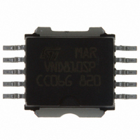
IC DRIVER 2CH HI-SIDE POWERSO-10
Manufacturer
STMicroelectronics
Type
High Sider
Datasheet
1.VND810SP.pdf
(27 pages)
Specifications of VND810SP
Input Type
Non-Inverting
Number Of Outputs
2
On-state Resistance
160 mOhm
Current - Peak Output
5A
Voltage - Supply
5.5 V ~ 36 V
Mounting Type
Surface Mount
Package / Case
PowerSO-10 Exposed Bottom Pad
Supply Voltage (min)
5.5 V
Supply Current
40 mA
Maximum Power Dissipation
52000 mW
Maximum Operating Temperature
+ 150 C
Mounting Style
SMD/SMT
Minimum Operating Temperature
- 40 C
Lead Free Status / RoHS Status
Contains lead / RoHS non-compliant
Operating Temperature
-
Current - Output / Channel
-
Lead Free Status / Rohs Status
Lead free / RoHS Compliant
Other names
497-3305-5
Available stocks
Company
Part Number
Manufacturer
Quantity
Price
Company:

Part Number:
VND810SP
Manufacturer:
VIA
Quantity:
1 831
Part Number:
VND810SP
Manufacturer:
ST
Quantity:
20 000
Company:
Part Number:
VND810SP13TR
Manufacturer:
TECHWELL
Quantity:
1 200


Application information
3
3.1
3.1.1
16/27
Application information
Figure 24. Application schematic
GND protection network against reverse battery
This section provides two solutions for implementing a ground protection network against
reverse battery.
Solution 1: a resistor in the ground line (R
This can be used with any type of load.
The following show how to dimension the R
1.
2.
where - I
maximum rating section of the device datasheet.
Power dissipation in R
This resistor can be shared amongst several different HSDs. Please note that the value of
this resistor should be calculated with formula (1) where I
maximum on-state currents of the different devices.
R
R
P
D
+5V
GND
GND
C
= ( -V
GND
600 mV / 2 (I
is the DC reverse ground pin current and can be found in the absolute
CC
-V
R
R
R
R
)
CC
prot
prot
prot
prot
2
/ R
) / ( -I
+5V
GND
GND
+5V
GND
S(on)max
(when V
)
STATUS1
INPUT1
STATUS2
INPUT2
Doc ID 7377 Rev 4
)
CC
< 0 during reverse battery situations) is:
V
GND
GND
resistor:
R
GND
GND
GND
V
S(on)max
CC
D
only)
GND
OUTPUT2
OUTPUT1
becomes the sum of the
VND810SP
D
ld
Related parts for VND810SP
Image
Part Number
Description
Manufacturer
Datasheet
Request
R

Part Number:
Description:
IC DRVR HISIDE 2CH 16-SOIC
Manufacturer:
STMicroelectronics
Datasheet:
Part Number:
Description:
IC DRIVER HIGH SIDE 2CH 16-SOIC
Manufacturer:
STMicroelectronics
Datasheet:

Part Number:
Description:
STMicroelectronics [RIPPLE-CARRY BINARY COUNTER/DIVIDERS]
Manufacturer:
STMicroelectronics
Datasheet:
Part Number:
Description:
STMicroelectronics [LIQUID-CRYSTAL DISPLAY DRIVERS]
Manufacturer:
STMicroelectronics
Datasheet:

Part Number:
Description:
BOARD EVAL FOR MEMS SENSORS
Manufacturer:
STMicroelectronics
Datasheet:
Part Number:
Description:
NPN TRANSISTOR POWER MODULE
Manufacturer:
STMicroelectronics
Datasheet:
Part Number:
Description:
TURBOSWITCH ULTRA-FAST HIGH VOLTAGE DIODE
Manufacturer:
STMicroelectronics
Datasheet:
Part Number:
Description:
Manufacturer:
STMicroelectronics
Datasheet:
Part Number:
Description:
DIODE / SCR MODULE
Manufacturer:
STMicroelectronics
Datasheet:
Part Number:
Description:
DIODE / SCR MODULE
Manufacturer:
STMicroelectronics
Datasheet:
Part Number:
Description:
Search -----> STE16N100
Manufacturer:
STMicroelectronics
Datasheet:
Part Number:
Description:
Search ---> STE53NA50
Manufacturer:
STMicroelectronics
Datasheet: