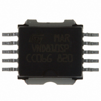
VND810SP STMicroelectronics, VND810SP Datasheet - Page 9

VND810SP
Manufacturer Part Number
VND810SP
Description
IC DRIVER 2CH HI-SIDE POWERSO-10
Manufacturer
STMicroelectronics
Type
High Sider
Datasheet
1.VND810SP.pdf
(27 pages)
Specifications of VND810SP
Input Type
Non-Inverting
Number Of Outputs
2
On-state Resistance
160 mOhm
Current - Peak Output
5A
Voltage - Supply
5.5 V ~ 36 V
Mounting Type
Surface Mount
Package / Case
PowerSO-10 Exposed Bottom Pad
Supply Voltage (min)
5.5 V
Supply Current
40 mA
Maximum Power Dissipation
52000 mW
Maximum Operating Temperature
+ 150 C
Mounting Style
SMD/SMT
Minimum Operating Temperature
- 40 C
Lead Free Status / RoHS Status
Contains lead / RoHS non-compliant
Operating Temperature
-
Current - Output / Channel
-
Lead Free Status / Rohs Status
Lead free / RoHS Compliant
Other names
497-3305-5
Available stocks
Company
Part Number
Manufacturer
Quantity
Price
Company:
Part Number:
VND810SP
Manufacturer:
VIA
Quantity:
1 831
Part Number:
VND810SP
Manufacturer:
ST
Quantity:
20 000
Company:
Part Number:
VND810SP13TR
Manufacturer:
TECHWELL
Quantity:
1 200
VND810SP
Table 7.
Table 8.
Table 9.
Table 10.
dV
dV
Symbol
Symbol
Symbol
V
V
I
C
Symbol
V
LSTAT
OUT
OUT
V
I(hyst)
V
STAT
V
STAT
I
SCL
t
t
I
V
d(on)
d(off)
IH
ICL
IL
IH
IL
F
/dt
/dt
(on)
(off)
Status low output voltage
Status leakage current
Status pin Input capacitance Normal operation; V
Status clamp voltage
Input low level
Low level input current
Input high level
High level input current
Input hysteresis voltage
Input clamp voltage
V
Switching (V
Logic inputs
Status pin
Turn-on delay time
Turn-off delay time
Turn-on voltage slope
Turn-off voltage slope
CC
Forward on voltage
- output diode
Parameter
Parameter
Parameter
Parameter
CC
= 13 V; T
Doc ID 7377 Rev 4
R
edge to V
(see
R
edge to V
(see
R
to V
(see
R
to V
(see
- I
L
L
L
L
= 13
= 13
= 13
= 13
OUT
OUT
OUT
V
V
I
I
I
Normal operation; V
I
I
j
IN
IN
STAT
STAT
STAT
Figure
Figure
Figure
Figure
IN
IN
= 25 °C)
Test conditions
= 1 mA
= -1 mA
= 1.25 V
= 3.25 V
= 0.5 A; T
= 10.4 V
= 1.3 V
Test conditions
Test conditions
= 1.6 mA
= 1 mA
= -1 mA
OUT
OUT
from V
from V
from V
from V
Test conditions
5)
5)
5)
5)
= 1.3 V
= 11.7 V
OUT
IN
IN
OUT
j
= 150 °C
rising
falling
= 11.7 V
= 1.3 V
STAT
STAT
= 5 V
= 5 V
Min.
Min.
3.25
0.5
—
—
—
—
1
6
Electrical specifications
Min.
—
Min.
Figure 10
Figure 12
6
Typ.
Typ.
-0.7
See
See
6.8
30
30
Typ.
—
Typ. Max. Unit
-0.7
6.8
Max.
1.25
Max.
Max. Unit
10
0.6
8
100
—
—
—
—
0.5
10
8
Unit
Unit
V/µs
V/µs
µA
µA
µs
µs
V
V
V
V
V
µA
pF
V
9/27
V
V
V


