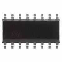
VND810-E STMicroelectronics, VND810-E Datasheet - Page 5

VND810-E
Manufacturer Part Number
VND810-E
Description
IC DRIVER HIGH SIDE 2CH 16-SOIC
Manufacturer
STMicroelectronics
Type
High Sider
Datasheet
1.VND810TR-E.pdf
(20 pages)
Specifications of VND810-E
Input Type
Non-Inverting
Number Of Outputs
2
On-state Resistance
160 mOhm
Current - Peak Output
5A
Voltage - Supply
5.5 V ~ 36 V
Mounting Type
Surface Mount
Package / Case
16-SOIC (3.9mm Width)
Switch Type
High Side
Power Switch Family
VND810
Power Switch On Resistance
160mOhm
Output Current
5A
Mounting
Surface Mount
Supply Current
12uA
Package Type
SO
Operating Temperature (min)
-40C
Operating Temperature (max)
150C
Operating Temperature Classification
Automotive
Pin Count
16
Power Dissipation
8.3W
Lead Free Status / RoHS Status
Lead free / RoHS Compliant
Operating Temperature
-
Current - Output / Channel
-
Lead Free Status / Rohs Status
Compliant
Available stocks
Company
Part Number
Manufacturer
Quantity
Price
Company:
Part Number:
VND810-E
Manufacturer:
ST
Quantity:
1 192
ELECTRICAL CHARACTERISTICS (continued)
Table 8. Status Pin
Table 9. Switching (V
Table 10. Openload Detection
Table 11. Logic Input
dV
dV
Symbol
Symbol
Symbol
t
t
Symbol
V
V
I
C
DOL(on)
DOL(off)
OUT
OUT
LSTAT
V
V
t
t
V
I(hyst)
V
V
STAT
I
STAT
I
d(on)
d(off)
I
SCL
OL
IH
ICL
IL
OL
IH
IL
/dt
/dt
(on)
(off)
Input Low Level
Low Level Input Current
Input High Level
High Level Input Current
Input Hysteresis Voltage
Input Clamp Voltage
Status Low Output Voltage I
Status Leakage Current
Status Pin Input
Capacitance
Status Clamp Voltage
Openload ON State
Detection Threshold
Openload ON State
Detection Delay
Openload OFF State
Voltage Detection
Threshold
Openload Detection Delay
at Turn Off
Turn-on Delay Time
Turn-off Delay Time
Turn-on Voltage Slope
Turn-off Voltage Slope
Parameter
Parameter
Parameter
Parameter
CC
=13V)
Normal Operation; V
Normal Operation; V
I
I
R
V
R
V
R
V
R
V
V
I
V
STAT
STAT
STAT
V
V
I
I
OUT
IN
IN
OUT
OUT
OUT
OUT
L
L
L
L
IN
IN
IN
IN
=13 from V
=13 from V
=13 from V
=13 from V
=5V
=0V
= 1mA
= -1mA
= 1.25V
= 3.25V
=0A
= 1.6 mA
= 1mA
= - 1mA
=1.3V
=11.7V
=10.4V
=1.3V
Test Conditions
Test Conditions
Test Conditions
Test Conditions
IN
IN
OUT
OUT
rising edge to
falling edge to
=1.3V to
=11.7V to
STAT
STAT
= 5V
= 5V
Min
Min
Min
1.5
3.25
20
Min
0.5
6
1
6
diagram
diagram
relative
relative
Typ
Typ
See
See
Typ
-0.7
2.5
Typ
-0.7
6.8
30
30
40
6.8
1000
Max
Max
Max
200
Max
1.25
100
3.5
0.5
80
10
10
8
VND810-E
8
V/ s
V/ s
Unit
Unit
Unit
Unit
mA
pF
V
V
V
V
V
V
V
V
V
s
s
A
A
A
s
s
5/20


