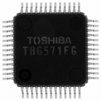
TB6571FG(O,EL) Toshiba, TB6571FG(O,EL) Datasheet - Page 10

TB6571FG(O,EL)
Manufacturer Part Number
TB6571FG(O,EL)
Description
IC DC MOTOR CTRLR BRUSHLSS 52QFP
Manufacturer
Toshiba
Specifications of TB6571FG(O,EL)
Applications
DC Motor Controller, Brushless (BLDC), 3 Phase
Number Of Outputs
1
Voltage - Supply
10 V ~ 28 V
Operating Temperature
-30°C ~ 85°C
Mounting Type
Surface Mount
Package / Case
52-QFP
Mounting Style
SMD/SMT
Lead Free Status / RoHS Status
Lead free / RoHS Compliant
Current - Output
-
Voltage - Load
-
Lead Free Status / Rohs Status
Lead free / RoHS Compliant
Other names
TB6571FGTR
Available stocks
Company
Part Number
Manufacturer
Quantity
Price
Generating an Internal Reference Clock
Generating Triangular Waves
Dead time Setup Circuit
Charge Pump
Motor Output Pins
The TB6571FG compares the modulation waveforms with triangular waves to generate PWM signals.
The carrier frequency for PWM control depends on the frequency of the triangular waves.
The triangular waves are switched according to the internal reference clock frequency.
The following formula obtains the PWM frequency, where fx2 is the internal reference clock frequency:
To apply PWM control with synchronous regeneration for output FETs, the TB6571FG sets a dead time for
energization signal outputs, thus preventing the upper and lower output power FETs from turning on
simultaneously.
It uses the internal reference clock, generated from external CR, to set a dead time.
The following formula obtains the dead time, where fx2 is the internal reference clock frequency:
The TB6571FG incorporates a charge pump to drive two N-ch FETs in the external output FET configuration,
in particular, to generate the gate voltage for the upper N-ch FET.
The booster voltage is V
The charge pump boosts the voltage using a frequency that is 1/16 of the internal reference clock frequency, fx2
(250 kHz when fx2 = 4 MHz).
Dead Time
The TB6571FG uses external C and R to generate a reference clock internally.
It uses the reference clock to generate triangular waves, which determine the carrier frequency, and set a
dead time.
The clock also functions as a reference clock for the charge pump (booster) and lead angle circuit ADC.
PWM frequency fpwm = fx2/252 (= triangular wave frequency)
For example: When fx2 = 5 MHz: fpwm = 19.8 kHz
Dead time td = (1/fx2) × 4
For example: When fx2 = 5 MHz: td = 0.8 µs
During PWM operation, the source voltage for the upper external N-ch FET swings between GND and VM.
VGS for the Nch-FET is clamped so that it does not exceed VGS (max) = 20 V.
(LB (U), LC (U) )
(LB (L), LC (L) )
LA (U)
LA (L)
When fx2 = 4 MHz: fpwm = 15.8 kHz
When fx2 = 3 MHz: fpwm = 11.9 kHz
When fx2 = 4 MHz: td = 1.0 µs
When fx2 = 3 MHz: td = 1.3 µs
CC
+ 8.0 V and the upper gate drive voltage is V
TOFF
10
TOFF
CC
+ 7.75 V.
TB6571FG
2005-04-15


