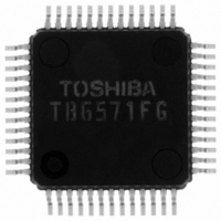
TB6571FG(O,EL) Toshiba, TB6571FG(O,EL) Datasheet - Page 3

TB6571FG(O,EL)
Manufacturer Part Number
TB6571FG(O,EL)
Description
IC DC MOTOR CTRLR BRUSHLSS 52QFP
Manufacturer
Toshiba
Specifications of TB6571FG(O,EL)
Applications
DC Motor Controller, Brushless (BLDC), 3 Phase
Number Of Outputs
1
Voltage - Supply
10 V ~ 28 V
Operating Temperature
-30°C ~ 85°C
Mounting Type
Surface Mount
Package / Case
52-QFP
Mounting Style
SMD/SMT
Lead Free Status / RoHS Status
Lead free / RoHS Compliant
Current - Output
-
Voltage - Load
-
Lead Free Status / Rohs Status
Lead free / RoHS Compliant
Other names
TB6571FGTR
Available stocks
Company
Part Number
Manufacturer
Quantity
Price
Pin Functions
Pin No.
10
11
12
13
14
15
16
17
18
19
20
21
22
23
24
25
26
27
28
29
30
31
32
33
34
35
36
37
38
39
40
1
2
3
4
5
6
7
8
9
PLL-GAIN
CW/CCW
BRAKE
LA (U1)
LA (U2)
LC (L1)
START
S-GND
P-GND
Ready
FGin+
FGin−
Name
Vref1
Vref2
VCO
HC+
HC−
FGS
VDD
VCC
HA+
HA−
HB+
HB−
FGo
CLd
CP1
CP2
CP3
Idc2
Idc1
Fref
Td1
Td2
LP1
NC
CP
L1
L2
L3
Phase-A hall signal input + pin
Phase-A hall signal input - pin
Phase-B hall signal input + pin
Phase-B hall signal input - pin
Phase-C hall signal input + pin
Phase-C hall signal input - pin
FG amplifier input + pin
FG amplifier input - pin
FG amplifier output pin
Forward/reverse switching pin
Brake
Start
External clock input
FG hysteresis comparator output pin
5-V reference power supply
PLL gain adjustment pin
Charge pump pin for speed control
Capacitor pin for VCO
Frequency setting pin 1 for internal
reference clock
Frequency setting pin 2 for internal
reference clock
Lead angle correction circuit
Lead angle correction circuit
Lead angle correction circuit
Internal logic power supply pin
8-V reference power supply
Input pin for output current detection signal GND sense pin
Input pin for output current detection signal Gate block operation when 0.25 V (typ.) or higher
Phase-C energization signal output (L1)
No connection
Ready output pin
Ground pin
For LPF
Oscillation pin for lock protection circuit
Ground pin
Charge pump pin
Charge pump pin
Charge pump pin
Voltage input pin for control power supply
Phase-A energization signal output (U1)
Phase-A energization signal output (U2)
Pin Functions
3
Input the positive phase-A Hall device signal.
Input the positive phase-B Hall device signal.
Pull-up resistor, L for start, H for standby
Pull-up resistor
Connect an external resistor for adjusting the correction gain.
Connect an external resistor for adjusting the correction gain.
Connect to GND through a capacitor.
For source driving for phase-C output FET gate (lower N-ch)
Input the negative phase-A Hall device signal.
Input the negative phase-B Hall device signal.
Input the positive phase-C Hall device signal.
Input the negative phase-C Hall device signal.
FG signal input
FG signal input
H: Reverse/L: Forward
Pull-up resistor, L for braking (all-phase ON for lower circuit)
Open collector output, I
Open collector output.
Within ±6%: L, Otherwise: High impedance
5-V output. Connect to GND through a capacitor.
Connect a resistor.
Connect to GND through a capacitor.
Connect to GND through a capacitor.
Connect external CR to generate a reference clock.
Connect an external capacitor.
5-V output. Connect to GND through a capacitor.
8-V output. Connect to GND through a capacitor.
For generating upper N-ch FET gate voltage
For generating upper N-ch FET gate voltage
For generating upper N-ch FET gate voltage
V
For source driving for phase-A output FET gate (upper N-ch)
For sink driving for phase-A output FET gate (upper N-ch)
CC
(opr.) = 10~28 V
O
= 1 mA (max)
Remarks
TB6571FG
2005-04-15


