ISL6271ACRZ Intersil, ISL6271ACRZ Datasheet - Page 10
ISL6271ACRZ
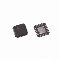
Manufacturer Part Number
ISL6271ACRZ
Description
IC REG PMIC 1BUCK 2LDO 20QFN
Manufacturer
Intersil
Datasheet
1.ISL6271ACRZ-T.pdf
(16 pages)
Specifications of ISL6271ACRZ
Applications
Processor
Current - Supply
380µA
Voltage - Supply
2.76 V ~ 5.5 V
Operating Temperature
-25°C ~ 85°C
Mounting Type
Surface Mount
Package / Case
20-QFN
Rohs Compliant
Yes
Lead Free Status / RoHS Status
Lead free / RoHS Compliant
Available stocks
Company
Part Number
Manufacturer
Quantity
Price

Part Number:
ISL6271ACRZ
Manufacturer:
INTERSIL
Quantity:
20 000
Part Number:
ISL6271ACRZ-T
Manufacturer:
INTERSIL
Quantity:
20 000
Company:
Part Number:
ISL6271ACRZT
Manufacturer:
INFN
Quantity:
5 195


BBAT
The BBAT pin is an input voltage to the ISL6271A that
supports the BFLT# indicator function as described above.
When the main battery is absent, or of inadequate potential,
the BBAT input voltage supplies power to support the BFLT#
indicator. The input voltage must be between 1.5V and
3.75V for proper operation and is typically supplied from the
system back-up battery. The maximum current drain from
the BBAT pin is 0.1µA.
PGOOD
PGOOD is an open-drain output that indicates the status of the
three regulators (VOUT, VSRAM, VPLL). This output is held
low until all outputs are within their specified voltage tolerance.
As soon as outputs are in regulation, the output is released and
pulled high by an external resistor tied to a compliant system
voltage. This output can be AND’d with other system power-
good indicators that also have open-drain outputs. Note that
this is not a latched output and under a soft short condition on
any of the regulators it is possible to see this pin oscillate at a
frequency proportional to the fault current level and the fault
monitoring hysteresis internal to the ISL6271A regulator.
PHASE Node Ring Damping Circuit
To enhance system reliability and minimize radiated
emission, the ISL6271A implements a PHASE node snubber
while operating in diode emulation. The active snubber
places a 50Ω (nominal) resistor across the output inductor
when the low side synchronous rectifier is turned off to
prevent reverse current.
Inter-IC Communications
Communication between the host processor and the
ISL6271A takes place over a two-wire I
consists of one bidirectional signal line, SDA (data), and a
clock pin input, SCL, generated by the bus master. Both pins
are pulled-high to a system voltage with external pull-up
resistors. A typical pull-up resistor value for a single
master/slave interface operating in normal mode is 5kΩ.
SDA
SCL
REPEATED START
CONDITION
START OR
OR
Sr
S
1
MSB
10
2
2
C interface. The bus
7
FIGURE 17. I
8
interrupt within slave
acknowledgement
signal from slave
byte complete,
ISL6271A
ACK
9
2
C DATA AND CLOCK
clock line held low while
interrupts are serviced
See the Phillips specification listed in the reference section for
specific details on the selection of the pull-up resistor. The bus
supports both standard mode and fast mode data rates as
defined by the Phillips protocol. A typical I
illustrated in Figure 17. When the bus-resident master
(processor) wants to communicate with a bus-resident slave
(ISL6271A), it will pull the SDA line low while the SCL line is
still high. This signals a “start” condition. It will then clock the
address of the desired slave device at a rate of one bit per
clock cycle. The address is embedded in the first seven bits of
the first byte transfer, with the eighth bit giving the directional
information (Read/Write) for the next byte of information.
When the slave detects an address match, it will hold the SDA
line low during the ninth clock pulse to acknowledge a match
(ACK). If the direction bit indicates a “write” (send) byte, the
slave will receive the byte clocked in by the master and will
give an “acknowledge” by again pulling the SDA line low
during the ninth clock cycle. The master then can either
terminate transmission by issuing a “stop” bit, or continue to
transfer successive bytes until complete.
Multiple successive bytes can be transferred with only an
acknowledge bit separating them until a “stop” or repeated
“start” signal is given by the master. The data embedded in
the byte is latched into its appropriate register(s) on the rising
edge of the SCL during the acknowledge pulse and is applied
to the ISL6271A DAC. The internal DAC on the ISL6271A
converts the 4 bit digital input as defined in Table 1 into the
reference voltage of the core regulator error amplifier.
If the master issues a ‘read’ command to the ISL6271A, to
verify the contents of the internal registers, the device will
place the byte on the bus to be clocked in by the master.
After the host master receives the byte, the cycle is
terminated by a “NOT acknowledge” signal, and a ‘stop’ bit.
A ‘stop’ is generated by releasing the SDA line to pull high
during a high state on the SCL line.
1
2
3-8
signal from receiver
acknowledgement
ACK
9
REPEATED START
CONDITION
2
STOP OR
C transmission is
OR
Sr
Sr
P
P
FN9171.1
Related parts for ISL6271ACRZ
Image
Part Number
Description
Manufacturer
Datasheet
Request
R

Part Number:
Description:
Intersil Corporation [CMOS Serial Controller Interface]
Manufacturer:
Intersil Corporation
Datasheet:
Part Number:
Description:
Manufacturer:
Intersil Corporation
Datasheet:
Part Number:
Description:
357-036-542-201 CARDEDGE 36POS DL .156 BLK LOPRO
Manufacturer:
Intersil Corporation
Datasheet:
Part Number:
Description:
1024-Word x 4-Bit LSI Static RAM
Manufacturer:
Intersil Corporation
Datasheet:
Part Number:
Description:
General Purpose NPN Transistor Arrays FN341.4
Manufacturer:
Intersil Corporation
Datasheet:
Part Number:
Description:
CMOS 16-Bit Microprocessor
Manufacturer:
Intersil Corporation
Datasheet:
Part Number:
Description:
Manufacturer:
Intersil Corporation
Datasheet:
Part Number:
Description:
Manufacturer:
Intersil Corporation
Datasheet:
Part Number:
Description:
Manufacturer:
Intersil Corporation
Datasheet:
Part Number:
Description:
Manufacturer:
Intersil Corporation
Datasheet:
Part Number:
Description:
CMOS 6-Bit Latch and Decoder Memory Interfaces
Manufacturer:
Intersil Corporation
Datasheet:
Part Number:
Description:
CA3046General Purpose NPN Transistor Arrays
Manufacturer:
Intersil Corporation
Datasheet:
Part Number:
Description:
Manufacturer:
Intersil Corporation
Datasheet:
Part Number:
Description:
TR909 DLC/FLC SLIC with Low Power Standby
Manufacturer:
Intersil Corporation
Datasheet:
Part Number:
Description:
Manufacturer:
Intersil Corporation
Datasheet: