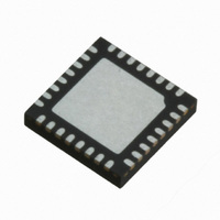
IR3529MTRPBF International Rectifier, IR3529MTRPBF Datasheet

IR3529MTRPBF
Specifications of IR3529MTRPBF
Related parts for IR3529MTRPBF
IR3529MTRPBF Summary of contents
Page 1
DESCRIPTION The IR3529 Phase IC combined with an IR XPhase3 implement power solutions for the latest high performance CPUs and ASICs. The “Control” IC provides overall system control and interfaces with any number of “Phase” ICs which each drive and ...
Page 2
... VCCL EAIN ISHARE 1 ILL ILL 2 PSI# PSI# 3 DACIN DACIN 4 LGND 5 PHSIN PHSIN SHIFT PHSOUT CLKIN ORDERING INFORMATION Part Number IR3529MTRPBF * IR3529MPBF * Samples only Page ROCSET COCSET GATEH 13 IR3529 BOOST 12 CBST VCCL 11 OCSET CVCCL1 Figure 1 Single Phase Application Circuit Package 20 Lead MLPQ ...
Page 3
ABSOLUTE MAXIMUM RATINGS Stresses beyond those listed under “Absolute Maximum Ratings” may cause permanent damage to the device. These are stress ratings only and functional operation of the device at these or any other conditions beyond those indicated in the ...
Page 4
RECOMMENDED OPERATING CONDITIONS FOR RELIABLE OPERATION WITH MARGIN 8.0V ≤ V ≤ 16V, 4.75V ≤ CCL 250kHz ≤ PHSIN ≤1.5MHz. ELECTRICAL CHARACTERISTICS The electrical characteristics involve the spread of values guaranteed within the recommended operating conditions. Typical values ...
Page 5
PARAMETER SW Floating Voltage Measured in the application with the converter not switching. Measure after 50us of CLKIN=0 with CSINM shorted to SW Calibrated Input Offset CSIN+ = CSIN- = DACIN. Measure input Voltage referred offset from DACIN. Note1 GAIN ...
Page 6
PARAMETER OVP Comparator OVP Threshold Propagation Delay Synchronous Rectification Disable Comparator Threshold Voltage Over Current Comparator IOCSET Sink Current Propagation Delay Time Turbo Comparator Activation Threshold Voltage Turbo Pulse Width Turbo Enable Threshold Debug Comparator Threshold Voltage General VCC Supply ...
Page 7
PIN DESCRIPTION PIN# PIN SYMBOL PIN DESCRIPTION 1 ILL Output of the Current Sense Amplifier is connected to this pin through a 3k resistor. Voltage on this pin is equal to V(DACIN [V(CSIN+) – V(CSIN-)]. Connecting all ILL ...
Page 8
SYSTEM THEORY OF OPERATION System Description The system consists of one control IC and a scalable array of phase converters, each requiring one phase IC. The control IC communicates with the phase ICs using three digital buses, i.e., CLOCK, PHSIN, ...
Page 9
Frequency and Phase Timing Control The oscillator is located in the Control IC and the system clock frequency is programmable from 250 kHz to 9 MHz by an external resistor. The control IC system clock signal (CLKOUT) is connected to ...
Page 10
PHASE IC CLOCK PULSE EAIN PWMRMP VDAC GATEH GATEL STEADY-STATE OPERATION TM Body Braking In a conventional synchronous buck converter, the minimum time required to reduce the current in the inductor in response to a load step decrease is; The ...
Page 11
Usually the resistor Rcs and capacitor Ccs are chosen so that the time constant of Rcs and Ccs equals the time constant of the inductor which is the inductance L over the inductor DCR (R voltage across Ccs is proportional ...
Page 12
PWM ramp thereby decreasing its duty cycle and output current. The current share amplifier is internally compensated so that the crossover frequency of the current share ...
Page 13
A synchronous rectification disable comparator is used to detect the converter’s CSIN- pin voltage, which represents local converter output voltage. If the voltage is below 75% of VDAC and negative current is detected, GATEL is driven low, which disables synchronous ...
Page 14
Turbo Modulator The turbo functionality is included in IR3529 to improve the transient performance of the system with reduced output capacitance. The turbo modulator consists of a comparator that monitors the EAIN signal and its filtered version. The modulator turns ...
Page 15
OUTPUT OVP VOLTAGE THRESHOLD (VO) VCCL-800 mV IOUT(ISHARE) GATEH (PHASE IC) GATEL (PHASE IC) FAULT LATCH ERROR AMPLIFIER VDAC OUTPUT (EAOUT) Over Voltage Protection (OVP) The IR3529 includes over-voltage protection that turns on the low side MOSFET to protect the ...
Page 16
APPLICATIONS SCHEMATIC +12V 4.75V to 7.5V VCCL PSI# VRRDY RMON IOUT RMON1 CMON CVCCL VOSEN- 33 EXPAD 1 24 VID7 VID7 PSI VID6 VID6 ROSC 3 22 VID5 VID5 SS/DEL 4 21 VID4 VID4 VDAC IR3503 5 20 ...
Page 17
DESIGN PROCEDURES - IR3529 Inductor Current Sensing Capacitor C The DC resistance of the inductor is utilized to sense the inductor current. Usually the resistor parallel with the inductor are chosen to match the time constant of ...
Page 18
LAYOUT GUIDELINES The following layout guidelines are recommended to reduce the parasitic inductance and resistance of the PCB layout; therefore, minimizing the noise coupled to the IC. • Dedicate at least one middle layer for a ground plane, which is ...
Page 19
PCB Metal and Component Placement • Lead land width should be equal to nominal part lead width. The minimum lead to lead spacing should be ≥ 0.2mm to minimize shorting. • Lead land length should be equal to maximum part ...
Page 20
Solder Resist • The solder resist should be pulled away from the metal lead lands and center pad by a minimum of 0.06mm. The solder resist mis-alignment is a maximum of 0.05mm and it is recommended that the lead lands ...
Page 21
Stencil Design • The stencil apertures for the lead lands should be approximately 80% of the area of the lead lands. Reducing the amount of solder deposited will minimize the occurrence of lead shorts. Since for 0.5mm pitch devices the ...
Page 22
PACKAGE INFORMATION 20L MLPQ ( Body) – θ IR WORLD HEADQUARTERS: 233 Kansas St., El Segundo, California 90245, USA Tel: (310) 252-7105 Visit us at www.irf.com for sales contact information. Page ...


