IR3529MTRPBF International Rectifier, IR3529MTRPBF Datasheet - Page 7
IR3529MTRPBF
Manufacturer Part Number
IR3529MTRPBF
Description
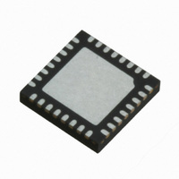
IC CTRL XPHASE CPU/ASIC 20-MLPQ
Manufacturer
International Rectifier
Series
XPhase3™r
Datasheet
1.IR3529MTRPBF.pdf
(22 pages)
Specifications of IR3529MTRPBF
Applications
Processor
Current - Supply
2mA
Voltage - Supply
8 V ~ 16 V
Operating Temperature
0°C ~ 125°C
Mounting Type
Surface Mount
Package / Case
*
Package
20-Lead MLPQ
Circuit
X-Phase Phase IC
Iout (a)
4.0A Gate Driver
Pbf
PbF Option Available
Lead Free Status / RoHS Status
Lead free / RoHS Compliant
Other names
IR3529MTRPBFTR


PIN DESCRIPTION
PIN#
10
11
12
13
14
15
16
17
18
19
20
1
2
3
4
5
6
7
8
9
Page 7 of 22
PIN SYMBOL
PHSOUT
ISHARE
BOOST
OCSET
GATEH
GATEL
DACIN
PHSIN
CLKIN
CSIN+
SHIFT
PGND
LGND
CSIN-
VCCL
EAIN
PSI#
VCC
SW
ILL
PIN DESCRIPTION
Output of the Current Sense Amplifier is connected to this pin through a 3k
resistor. Voltage on this pin is equal to V(DACIN) + 33 [V(CSIN+) – V(CSIN-)].
Connecting all ILL pins together creates a bus which provides an indication of the
average current being supplied by the power supply. The signal is used by the
Control IC for voltage positioning and over-current protection. OVP mode is initiated
if the voltage on this pin rises above V(VCCL)- 0.8V.
Digital Power State Indicator input, active low.
Reference voltage input from the Control IC. The Current Sense signal and PWM
ramp is referenced to the voltage on this pin.
Ground for internal IC circuits. IC substrate is connected to this pin.
Phase clock input at switching frequency.
Communication input from phase IC(s) statically floats at VCCL/2. Momentarily
pulling pin up to VCCL indicates a phase has entered the daisy chain loop resulting
in an up-shift in the CLKOUT frequency. Momentarily pulling down to ground
indicates a loss of a phase and down-shifts the CLKOUT frequency.
Phase clock output at switching frequency.
Clock input.
Return for low side driver and reference for GATEH non-overlap comparator.
Low-side driver output and input to GATEH non-overlap comparator.
Programs cycle by cycle Over Current threshold voltage. V(OCSET) gets compared
against the V(SW) node when the high side MOSFET is on. If V(SW) gets below
V(OCSET), the next switch pulse gets skipped to allow inductor relaxation. The
V(OCSET) threshold is programmed by forcing a 200uA current sink through an
external resistor kelvined to the drain of the high side FET.
Supply for low-side driver. Internal bootstrap synchronous PFET is connected from
this pin to the BOOST pin.
Supply for high-side driver. Internal bootstrap synchronous PFET is connected
between this pin and the VCCL pin.
High-side driver output and input to GATEL non-overlap comparator.
Return for high-side driver and reference for GATEL non-overlap comparator.
Supply for internal IC circuits.
Non-Inverting input to the current sense amplifier, and input to debug comparator.
Inverting input to the current sense amplifier, and input to synchronous rectification
disable comparator.
PWM comparator input from the error amplifier output of Control IC. Body Braking
mode is initiated if the voltage on this pin is less than V(DACIN).
Output of the Current Sense Amplifier is connected to this pin through a 3k
resistor. Voltage on this pin is equal to V(DACIN) + 33 [V(CSIN+) – V(CSIN-)].
Connecting all ISHARE pins together creates a share bus which provides an
indication of the average current being supplied by active phases only. The pin
becomes high impedance during PSI# activation.
February 12, 2010
IR3529
Related parts for IR3529MTRPBF
Image
Part Number
Description
Manufacturer
Datasheet
Request
R

Part Number:
Description:
SCHOTTKY RECTIFIER
Manufacturer:
International Rectifier Corp.
Datasheet:
Part Number:
Description:
SCHOTTKY RECTIFIER
Manufacturer:
International Rectifier Corp.
Datasheet:
Part Number:
Description:
SCHOTTKY RECTIFIER
Manufacturer:
International Rectifier Corp.
Datasheet:
Part Number:
Description:
SCHOTTKY RECTIFIER
Manufacturer:
International Rectifier Corp.
Datasheet:
Part Number:
Description:
SCHOTTKY RECTIFIER
Manufacturer:
International Rectifier Corp.
Datasheet:
Part Number:
Description:
SCHOTTKY RECTIFIER
Manufacturer:
International Rectifier Corp.
Datasheet:
Part Number:
Description:
SCHOTTKY RECTIFIER
Manufacturer:
International Rectifier Corp.
Datasheet:
Part Number:
Description:
SCHOTTKY RECTIFIER
Manufacturer:
International Rectifier Corp.
Datasheet:
Part Number:
Description:
SCHOTTKY RECTIFIER
Manufacturer:
International Rectifier Corp.
Datasheet:
Part Number:
Description:
SCHOTTKY RECTIFIER
Manufacturer:
International Rectifier Corp.
Datasheet:
Part Number:
Description:
SCHOTTKY RECTIFIER
Manufacturer:
International Rectifier Corp.
Datasheet:
Part Number:
Description:
SCHOTTKY RECTIFIER
Manufacturer:
International Rectifier Corp.
Datasheet:
Part Number:
Description:
SCHOTTKY RECTIFIER
Manufacturer:
International Rectifier Corp.
Datasheet:
Part Number:
Description:
SCHOTTKY RECTIFIER
Manufacturer:
International Rectifier Corp.
Datasheet:
Part Number:
Description:
SCHOTTKY RECTIFIER
Manufacturer:
International Rectifier Corp.
Datasheet: