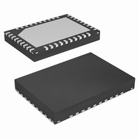
ISL24006IRZ-T7 Intersil, ISL24006IRZ-T7 Datasheet - Page 7

ISL24006IRZ-T7
Manufacturer Part Number
ISL24006IRZ-T7
Description
IC VOLT GEN I2C 14-CH 38-QFN
Manufacturer
Intersil
Datasheet
1.ISL24006IRZ.pdf
(10 pages)
Specifications of ISL24006IRZ-T7
Applications
LCD Drive, Reference Voltage Generator
Current - Supply
30mA
Voltage - Supply
5 V ~ 18 V
Operating Temperature
-40°C ~ 85°C
Mounting Type
Surface Mount
Package / Case
38-VQFN Exposed Pad, 38-HVQFN, 38-SQFN, 38-DHVQFN
Lead Free Status / RoHS Status
Lead free / RoHS Compliant
For the Standard mode in a READ transfer, a master device
accepts data from the ISL24006. The output data byte
(DATA 1) of the first channel (OUT1) is the second byte of
the transfer. OUT2 output data byte is the third byte of the
transfer, and so forth and so on. The ISL24006 sends an
acknowledge bit after every eighth bit to tell the master
device that the ISL24006 is ready to send another byte.
Consequently, the master must send a Not Acknowledge,
(NA) at the end of the 14th data byte to tell ISL24006 to
release the SDA bus.
See Timing Diagram 1 (Figure 1) for detailed formats.
Devices Address and W/R Bit
Data transfers follow the format shown in Timing Diagram 1.
After the Start condition, a first byte is sent which contains
the Device Address and write/read bit. This address is a 7-bit
long device address and only two device addresses hex (74)
and hex (75) in binary, bin (111010) and bin (111011) are
allowed for the ISL24006. The first 6 bits (A6 to A1, MSBs) of
the device address have been factory programmed and are
always 111010. Only the least significant bit (LSB) A0 is
allowed to change the logic state. This LSB is controlled
externally on the pin #4, A0. When pulled high to D
LSB of the device address is high and thus the address is
hex (75) or in binary bin (1110101). When pulled low to GND,
the LSB of the device address low and thus the address is
hex (74) or in binary 1110100. Since the device address has
to be unique in the I
may be used on the same bus at one time.
The ISL24006 monitors the bus continuously and waiting for
the Start condition followed by the device address. When the
device recognizes its device address, it will start to accept
data. The eighth bit (W/R) following the device address
indicates the data direction. A "0" is a Write transmission; a
master device will send data to the ISL24006 to set or
S = Start condition
P = Stop condition
S = Start condition
P = Stop condition
A = Acknowledge bit
S
S
ADDRESS + R A DATA 1 A DATA 2 A ...
ISL24006 ADDRESS + W
ISL24006
TABLE 2. Standard Mode READ Transfer
2
A = Acknowledge
NA = Not Acknowledge
DATA 1 = 8-bit input to DAC OUT1
DATA 2 = 8-bit input to DAC OUT2
DATA 14 = 8-bit input to DAC OUT14
C bus line, a maximum of two ISL24006
7
A
CONTROL BYTE = multifunction control
DATA 1 = 8-bit input to DAC OUT1
DATA 2 = 8-bit input to DAC OUT2
DATA 14 = 8-bit input to DAC OUT14
CONTROL BYTE
TABLE 1. STANDARD MODE WRITE TRANSFER
DATA
VDD
14
, the
P
ISL24006
A
program a desired reference voltage. A "1" indicates a Read
transmission; the master device will receive data from the
ISL24006 to read the previous data the voltage reference
was set or programmed.
Control Byte
The multi-function control byte contains information that
selects the memory bank (bankA, or bankB), and operation
(output, read, or write). It also controls the OSC pin function
(external or internal).
The second bit, C1, selects which bank to write to. A "0"
selects bankA. A "1" selects bankB. C1 is a "don't care" on
a read mode.
The third bit, C2, selects which bank to read from. A "0"
selects bankA. A "1" selects bankB. C2 is a "don't care" on
a write mode.
The fourth bit, C3, selects the function of the OSC pin. A "0"
selects the internal oscillator. When the internal oscillator is
selected, the OSC pin acts as an output pin. It generates a
square wave with a frequency of typically 20kHz where
multiple chips can be synchronized. A "1" selects an external
oscillator. When the external oscillator is selected, the OSC
pin acts an input pin. Multiple chips can be synchronized to
an external oscillator. The external frequency or refresh rate
can be synchronized up to 200kHz typically.
The rest of the bits (C4-C7) in the control byte are "don't
cares".
DATA 1
C0
C1
C2
C3
C7
X
= "0" bypass oscillator
= "1" 3.5µs lagging
= "0" write data to bankA (default)
= "1" write data to bankB
= "0" read data from bankA (default)
= "1" read data from bankB
= "0" internal oscillator (default)
= "1" external oscillator
C6
X
A
C5
DATA 2
X
TABLE 3. Control Byte
C4
X
A
C3
0
...
DATA 14
C2
0
C1
0
March 9, 2006
A
FN6110.1
C0
0
P


