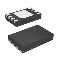
SE97BTP,547 NXP Semiconductors, SE97BTP,547 Datasheet - Page 19

SE97BTP,547
Manufacturer Part Number
SE97BTP,547
Description
IC TEMP SENSOR DIMM 8HWSON
Manufacturer
NXP Semiconductors
Datasheet
1.SE97BTP547.pdf
(53 pages)
Specifications of SE97BTP,547
Package / Case
8-WSON (Exposed Pad), 8-HWSON
Function
Temp Monitoring System (Sensor)
Topology
ADC (Sigma Delta), Comparator, Register Bank
Sensor Type
Internal
Sensing Temperature
-40°C ~ 125°C
Output Type
I²C™/SMBus™
Output Alarm
Yes
Output Fan
Yes
Voltage - Supply
3 V ~ 3.6 V
Operating Temperature
-40°C ~ 125°C
Mounting Type
Surface Mount
Temperature Threshold
+ 150 C
Full Temp Accuracy
2 C
Digital Output - Bus Interface
I2C
Digital Output - Number Of Bits
11 bit
Supply Voltage (max)
3.6 V
Supply Voltage (min)
3 V
Description/function
Temperature Sensor
Maximum Operating Temperature
+ 125 C
Minimum Operating Temperature
- 40 C
Lead Free Status / RoHS Status
Lead free / RoHS Compliant
Lead Free Status / RoHS Status
Lead free / RoHS Compliant, Lead free / RoHS Compliant
Other names
568-5055-2
NXP Semiconductors
Table 7.
Instructions with R/W bit = 0.
Table 8.
Instructions with R/W bit = 1.
SE97B_1
Product data sheet
Status
Permanently
protected
Protected with
RWP
Not protected
Status
Permanently
protected
Protected with
RWP
Not protected
Acknowledge when writing data or defining write protection
Acknowledge when reading the write protection
7.10.2.2 Reversible Write Protection (RWP) and Clear Reversible Write Protection (CRWP)
7.10.2.3 Read Permanent Write Protection (RPWP), Read Reversible Write Protection
PWP or RWP
RPWP, RRWP or
Instruction
PWP, RWP or CRWP
page or byte write in
lower 128 bytes
RWP
CRWP
PWP
page or byte write in
lower 128 bytes
CRWP
page or byte write
Instruction
RPWP, RRWP or
RCRWP
RRWP
RCRWP
RPWP
RCRWP
If the software write-protection has been set with the RWP instruction, it can be cleared
again with a CRWP instruction.
The two instructions, RWP and CRWP have the same format as a Byte Write instruction,
but with a different setting for the hardware address pins (as shown in
Byte Write instruction, it is followed by an address byte and a data byte, but in this case
the contents are all ‘Don’t Care’
must be applied on the A0 pin, and specific logical levels must be applied on the other two
(A1 and A2), as shown in
(RRWP), and Read Clear Reversible Write Protection (RCRWP)
Read PWP, RWP, and CRWP allow the SE97B to be read in write protection mode. The
instruction format is the same as that of the write protection except that the 8
set to 1.
the instructions are issued.
Figure 14
ACK
NACK
ACK
NACK
ACK
ACK
ACK
ACK
ACK
ACK
ACK
NACK
NACK
ACK
ACK
ACK
shows the instruction format, while
Rev. 01 — 27 January 2010
Table
not significant
not significant
not significant
address
not significant
not significant
Address
address
not significant
not significant
address
not significant
Address
not significant
not significant
not significant
DDR memory module temp sensor with integrated SPD
6.
(Figure
13). Another difference is that the voltage, V
NACK
ACK
NACK
ACK
ACK
ACK
NACK
NACK
ACK
ACK
ACK
ACK
ACK
NACK
NACK
NACK
Data byte
not significant
data
not significant
not significant
not significant
data
not significant
not significant
data
Data byte
not significant
not significant
not significant
not significant
not significant
Table 8
shows the responses when
NACK
NACK
ACK
NACK
NACK
NACK
NACK
NACK
ACK
NACK
ACK
ACK
ACK
ACK
ACK
NACK
Table
© NXP B.V. 2010. All rights reserved.
SE97B
th
6). Like the
no
no
yes
no
Write cycle
(t
no
yes
yes
no
yes
bit, R/W, is
W
)
19 of 53
I(ov)
,


